|
전자부품 데이터시트 검색엔진 |
|
|
전자부품 데이터시트 검색엔진 |
|
SC2453 데이터시트(PDF) 10 Page - Semtech Corporation |
|
|
|||||||||||||||||||||||||||||
SC2453 데이터시트(HTML) 10 Page - Semtech Corporation |
|
|
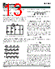
10 / 22 page  10 2005 Semtech Corp. www.semtech.com SC2453 POWER MANAGEMENT Applications Information (Cont.) Vdiode drop. Shoot through control circuitry provides a 30ns dead time to ensure both the upper and lower MOSFET will not turn on simultaneously and cause a shoot through condition. Error Amplifier and PWM Controller Error Amplifier and PWM Controller Error Amplifier and PWM Controller Error Amplifier and PWM Controller Error Amplifier and PWM Controller In closed loop operation, the internal oscillator ramp ranges from 0.75V to 3.8V. The error amplifier output ranges determines duty-ratio of a converter. The synchro- nous continuous-conduction mode of operation allows the SC2453 to regulate the output irrespective of the direction of the load current. The SC2453 uses voltage-mode control for good noise immunity and ease of compensation. The low-side MOSFET of each channel is turned off at the falling-edge of the phase timing clock. After a brief non-overlapping time interval of 30ns, the high-side MOSFET is turned on. The phase inductor current ramps up. When the in- ternal ramp reaches the threshold determined by the error amplifier output, the high-side MOSFET is turned off. As long as phase voltage collapses below 1.5V, the low-side MOSFET is turned on. Buck Converter Buck Converter Buck Converter Buck Converter Buck Converter Buck converter design includes the following specifica- tions: Input voltage range: ] V , V [ V max , in min , in in ∈ Input voltage ripple (peak-to-peak): ∆V in Output voltage: V o Output voltage accuracy: ε Output voltage ripple (peak-to-peak): ∆V o Nominal output (load) current: I o Maximum output current limit: I o,max Output (load) current transient slew rate: dI o (A/s) Circuit efficiency: η Selection criteria and design procedures for the following are described. 1) output inductor (L) type and value, 2) output capacitor (C o) type and value, 3) input capacitor (C in) type and value, 4) power MOSFET’s, 5) current sensing and limiting circuit, 6) voltage sensing circuit, 7) loop compensation network. Operating Frequency (f Operating Frequency (f Operating Frequency (f Operating Frequency (f Operating Frequency (f sssss))))) The switching frequency in the SC2453 is user- programmable. The advantages of using constant frequency operation are simple passive component selection and ease of feedback compensation. Before setting the operating frequency, the following trade-offs should be considered. 1) Passive component size 2) Circuitry efficiency 3) EMI condition 4) Minimum switch on time and 5) Maximum duty ratio For a given output power, the sizes of the passive components are inversely proportional to the switching frequency, whereas MOSFET’s/Diodes switching losses are proportional to the operating frequency. Other issues such as heat dissipation, packaging and the cost issues are also to be considered. The frequency bands for signal transmission should be avoided because of EM interference. Minimum Switch On Time Consideration Minimum Switch On Time Consideration Minimum Switch On Time Consideration Minimum Switch On Time Consideration Minimum Switch On Time Consideration In the SC2453, the falling edge of the clock turns on the top MOSFET. The inductor current and the sensed voltage ramp up. After the internal ramp voltage crosses a threshold determined by the error amplifier output, the top MOSFET is turned off. The propagation delay time from the turn-on of the controlling FET to its turn-off is the minimum switch on time. The SC2453 has a minimum on time of about 50ns at room temperature. This is the shortest on interval of the controlling FET. The controller either does not turn on the top MOSFET at all or turns it on for at least 50ns. For a synchronous step-down converter, the operating duty cycle is V O/VIN. So the required on time for the top MOSFET is V O/(VINfs). If the frequency is set such that the required pulse width is less than 50ns, then the converter will start skipping cycles. Due to minimum on time limitation, simultaneously operating at very high switching frequency and very short duty cycle is not practical. If the voltage conversion ratio V O/VIN and hence the required duty cycle is higher, the switching frequency can be increased to reduce the size of passive components. |
|
|
링크 URL |
| ALLDATASHEET 가 귀하에 도움이 되셨나요? [ DONATE ] |
Alldatasheet는? | 광고문의 | 운영자에게 연락하기 | 개인정보취급방침 | 링크 투 데이터시트 | 링크교환 | 제조사별 검색 All Rights Reserved©Alldatasheet.com |
| Russian : Alldatasheetru.com | Korean : Alldatasheet.co.kr | Spanish : Alldatasheet.es | French : Alldatasheet.fr | Italian : Alldatasheetit.com Portuguese : Alldatasheetpt.com | Polish : Alldatasheet.pl | Vietnamese : Alldatasheet.vn Indian : Alldatasheet.in | Mexican : Alldatasheet.com.mx | British : Alldatasheet.co.uk | New Zealand : Alldatasheet.co.nz |
|
Family Site : ic2ic.com |
icmetro.com |
 Korean ▼
 English
 Chinese
 German
 Japanese
 Russian
 Korean
 Spanish
 French
 Italian
 Portuguese
 Polish
 Vietnamese
 Indian
 Mexican
 British
 New Zealand