|
전자부품 데이터시트 검색엔진 |
|
|
전자부품 데이터시트 검색엔진 |
|
SC2453 데이터시트(PDF) 15 Page - Semtech Corporation |
|
|
|||||||||||||||||||||||||||||
SC2453 데이터시트(HTML) 15 Page - Semtech Corporation |
|
|
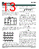
15 / 22 page  15 2005 Semtech Corp. www.semtech.com SC2453 POWER MANAGEMENT s in o 2 f r 2 1 ts f V I) 1 )( t t ( P δ + + = where t r is the rise time and tf is the fall time of the switching process. Different manufactures have different definitions and test conditions for t r and t f . To clarify these, we sketch the typical MOSFET switching characteristics under clamped inductive mode in Figure 6. Figure 6. MOSFET switching characteristics Where, Q gs1 is the gate charge needed to bring the gate-to-source voltage V gs to the threshold voltage Vgs_th, Q gs2 is the additional gate charge required for the switch current to reach its full-scale value I ds . and Q gd is the charge needed to charge gate-to-drain (Miller) capacitance when V ds is falling. Switching losses occur during the time interval [t 1, t3]. Defining t r = t3-t1 and tr can be approximated as: gsp cc gt gd 2 gs r V V R ) Q Q ( t − + = where R gt is the total resistance from the driver supply rail to the gate of the MOSFET. It includes the gate driver internal impedance R gi, external resistance Rge and the gate resistance R g within the MOSFET i.e.: R gt = Rgi+Rge+Rg V gsp is the Miller plateau voltage shown in Figure 11. Similarly an approximate expression for t f is: gsp gt gd 2 gs f V R ) Q Q ( t + = Only a portion of the total losses P g = QgVccfs is dissipated in the MOSFET package. Here Q g is the total gate charge specified in the datasheet. The power dissipated within the MOSFET package is: s cc g gt g tg f V Q R R P = The total power loss of the top switch is then: P t = Ptc+Pts+Ptg If the input supply of the power converter varies over a wide range, then it will be necessary to weigh the relative importance of conduction and switching losses. This is because conduction losses are inversely proportional to the input voltage. Switching loss how- ever increases with the input voltage. The total power loss of MOSFET should be calculated and compared for high-line and low-line cases. The worst case is then used for thermal design. Bottom Switch: The RMS current in bottom switch can be shown to be: ) 1 )( D 1 ( I I 12 o rms , 2 Q 2 δ + − = The conduction losses are then: P bc=IQ2,rms 2 R ds(on) where R ds(on) is the channel resistance of bottom MOSFET. If the input voltage to output voltage ratio is high (e.g. V in=12V, Vo=1.5V), the duty ratio D will be small. Since the bottom switch conducts with duty ratio (1-D), the corresponding conduction losses can be quite high. Due to non-overlapping conduction between the top and the bottom MOSFET’s, the internal body diode or the external Schottky diode across the drain and source terminals always conducts prior to the turn on of the bottom MOSFET. The bottom MOSFET switches on with only a diode voltage between its drain and source terminals. The switching loss is: s d o 2 f r 2 1 bs f V I) 1 )( t t ( P δ + + = is negligible due to near zero-voltage switching. The gate losses are estimated as : s cc g gt g bg f V Q R R P = The total bottom switch losses are then: P b=Pbc+Pbs+Pbg |
|
|
링크 URL |
| ALLDATASHEET 가 귀하에 도움이 되셨나요? [ DONATE ] |
Alldatasheet는? | 광고문의 | 운영자에게 연락하기 | 개인정보취급방침 | 링크 투 데이터시트 | 링크교환 | 제조사별 검색 All Rights Reserved©Alldatasheet.com |
| Russian : Alldatasheetru.com | Korean : Alldatasheet.co.kr | Spanish : Alldatasheet.es | French : Alldatasheet.fr | Italian : Alldatasheetit.com Portuguese : Alldatasheetpt.com | Polish : Alldatasheet.pl | Vietnamese : Alldatasheet.vn Indian : Alldatasheet.in | Mexican : Alldatasheet.com.mx | British : Alldatasheet.co.uk | New Zealand : Alldatasheet.co.nz |
|
Family Site : ic2ic.com |
icmetro.com |
 Korean ▼
 English
 Chinese
 German
 Japanese
 Russian
 Korean
 Spanish
 French
 Italian
 Portuguese
 Polish
 Vietnamese
 Indian
 Mexican
 British
 New Zealand