|
전자부품 데이터시트 검색엔진 |
|
|
전자부품 데이터시트 검색엔진 |
|
SC2453 데이터시트(PDF) 17 Page - Semtech Corporation |
|
|
|||||||||||||||||||||||||||||
SC2453 데이터시트(HTML) 17 Page - Semtech Corporation |
|
|
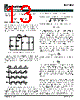
17 / 22 page  17 2005 Semtech Corp. www.semtech.com SC2453 POWER MANAGEMENT Where, T is switching cycle period. Because the inductor current ramps up according to Vin –Vo, and down with Vo, a falling output voltage in over current condition moves the inductor “ramp up” current up faster and the peak current I P larger but the “ramp down” current slower. As long as the current is still larger than the current limiting threshold, the top switch is held off. The switching frequency is folded back lower but average current is relatively still high. An example is shown in Typical Characteristics section with input voltage 12V and output voltage 5V with out- put current 3.5A. The preset valley current limit is 5A, which has to be greater than full load current 3.5. When the output is shorted, the inductor peak current and the load current, both are a function of the input voltage and the output inductance, would be higher than the current limit. There- fore, proper thermal management and inductor satura- tion current rating have to be considered at the worst conditions. Loop Compensation Loop Compensation Loop Compensation Loop Compensation Loop Compensation SC2453 is a voltage mode buck controller with high gain bandwidth error amplifier utilizing external network com- pensation to regulate output voltage. For a DC/DC converter, it is usually required that the converter has a loop gain of a high crossover frequency for fast load response, high DC and low frequency gain for low steady state error, and enough phase margin for its operating stability. Often one can not have all these properties at the same time. The purpose of the loop compensation is to arrange the poles and zeros of the compensation network to meet the requirements for a specific application. The power stage of a buck converter control-to-output transfer function is as shown below: LC s R L s 1 C sR 1 V ) s ( G 2 C IN VD + + + = where, LC 1 O = ω L - Output inductance C - Output capacitance R C - Output capacitor ESR V IN - Input voltage The transfer function of the error amplifier with external compensation network is as follows: ) s 1 )( s 1 ( ) s 1 )( s 1 ( s ) s ( G 2 P 1 P 2 Z 1 Z I COMP ω + ω + ω + ω + ⋅ ω = where, 2 3 1 2 Z 1 2 1 Z C ) R R ( 1 , C R 1 + = ω = ω 3 1 3 1 2 2 P 2 3 1 P 3 1 1 I C C C C R 1 , C R 1 , ) C C ( R 1 + = ω = ω + = ω R3 C3 R2 R1 C1 Vref C2 - + Figure 7. Voltage Mode Buck Converter Compensation Network With the compensation, the converter total loop gain is as follows: C L s R L s 1 C R 1 s 1 s 1 s 1 s 1 s 1 s V V 1 ) s ( G ) s ( G G ) s ( T 1 2 1 4 C 2 P 2 Z 1 P 1 Z I I M VD COMP PWM + + ⋅ + ⋅ ω + ⋅ ω + ⋅ ω + ω + ⋅ ⋅ ω ⋅ = ⋅ ⋅ = Where: G PWM = PWM gain V M = 3.0V, ramp peak to valley voltage of SC2453 The design guidelines are as following: 1. Set the loop gain crossover frequency ω C less than1/ 5th the switching frequency. 2. Place an integrator in the origin to increase DC and low frequency gains. |
|
|
링크 URL |
| ALLDATASHEET 가 귀하에 도움이 되셨나요? [ DONATE ] |
Alldatasheet는? | 광고문의 | 운영자에게 연락하기 | 개인정보취급방침 | 링크 투 데이터시트 | 링크교환 | 제조사별 검색 All Rights Reserved©Alldatasheet.com |
| Russian : Alldatasheetru.com | Korean : Alldatasheet.co.kr | Spanish : Alldatasheet.es | French : Alldatasheet.fr | Italian : Alldatasheetit.com Portuguese : Alldatasheetpt.com | Polish : Alldatasheet.pl | Vietnamese : Alldatasheet.vn Indian : Alldatasheet.in | Mexican : Alldatasheet.com.mx | British : Alldatasheet.co.uk | New Zealand : Alldatasheet.co.nz |
|
Family Site : ic2ic.com |
icmetro.com |
 Korean ▼
 English
 Chinese
 German
 Japanese
 Russian
 Korean
 Spanish
 French
 Italian
 Portuguese
 Polish
 Vietnamese
 Indian
 Mexican
 British
 New Zealand