|
전자부품 데이터시트 검색엔진 |
|
|
전자부품 데이터시트 검색엔진 |
|
ADBMS1818ASWAZ-R7 데이터시트(PDF) 88 Page - Analog Devices |
|
|
|||||||||||||||||||||||||||||
ADBMS1818ASWAZ-R7 데이터시트(HTML) 88 Page - Analog Devices |
|
|
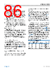
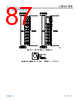
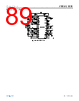
88 / 92 page  Data Sheet ADBMS1818 APPLICATIONS INFORMATION analog.com Rev. B | 88 of 92 READING EXTERNAL TEMPERATURE PROBES Figure 110 shows the typical biasing circuit for a negative tempera- ture coefficient (NTC) thermistor. The 10 kΩ at 25°C is the most popular sensor value and the VREF2 output stage is designed to provide the current required to bias several of these probes. The biasing resistor is selected to correspond to the NTC value so the circuit provides 1.5 V at 25°C (VREF2 is 3 V nominal). The overall circuit response is approximately –1%/°C in the range of typical cell temperatures, as shown in the chart of Figure 110. Expanding the Number of Auxiliary Measurements The ADBMS1818 has nine GPIO pins that can be used as ADC inputs. In applications that need to measure more than nine signals, a mux circuit can be implemented to expand the analog measure- ments to 16 different signals (Figure 111). The GPIO1 ADC input is used for measurement and mux control is provided by the I2C port on GPIO4 and GPIO5. The buffer amplifier is selected for fast settling and increases the usable throughput rate. Figure 110. Typical Temperature Probe Circuit and Relative Output Figure 111. Mux Circuit Supports 16 Additional Analog Measurements |
|
링크 URL |
| ALLDATASHEET 가 귀하에 도움이 되셨나요? [ DONATE ] |
Alldatasheet는? | 광고문의 | 운영자에게 연락하기 | 개인정보취급방침 | 링크 투 데이터시트 | 링크교환 | 제조사별 검색 All Rights Reserved©Alldatasheet.com |
| Russian : Alldatasheetru.com | Korean : Alldatasheet.co.kr | Spanish : Alldatasheet.es | French : Alldatasheet.fr | Italian : Alldatasheetit.com Portuguese : Alldatasheetpt.com | Polish : Alldatasheet.pl | Vietnamese : Alldatasheet.vn Indian : Alldatasheet.in | Mexican : Alldatasheet.com.mx | British : Alldatasheet.co.uk | New Zealand : Alldatasheet.co.nz |
|
Family Site : ic2ic.com |
icmetro.com |
 Korean ▼
 English
 Chinese
 German
 Japanese
 Russian
 Korean
 Spanish
 French
 Italian
 Portuguese
 Polish
 Vietnamese
 Indian
 Mexican
 British
 New Zealand