|
전자부품 데이터시트 검색엔진 |
|
|
전자부품 데이터시트 검색엔진 |
|
ADP1660ACBZ-R7 데이터시트(PDF) 24 Page - Analog Devices |
|
|
|||||||||||||||||||||||||||||
ADP1660ACBZ-R7 데이터시트(HTML) 24 Page - Analog Devices |
|
|
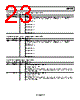
24 / 28 page  ADP1660 Data Sheet Rev. 0 | Page 24 of 28 APPLICATIONS INFORMATION EXTERNAL COMPONENT SELECTION Selecting the Inductor The ADP1660 boost converter increases the battery voltage to allow driving of two LEDs when the forward voltage of the LEDs is higher than the battery voltage minus 2× the current source headroom voltage. This allows the converter to regulate the LED current over the entire battery voltage range and with a wide variation of LED forward voltages. The inductor saturation current should be greater than the sum of the dc input current and half the inductor ripple current. A reduction in the effective inductance due to saturation increases the inductor ripple current. Table 28 provides a list of suggested inductors. Table 28. Suggested Inductors Vendor Value (µH) Part No. DCR (mΩ) ISAT (A) Dimensions L × W × H (mm) Toko 1.0 FDSD0312 43 4.5 3.0 × 3.0 × 1.2 Toko 1.0 DFE2520 50 3.4 2.5 × 2.0 × 1.0 Coilcraft 1.0 XFL3010 43 2.4 3.0 × 3.0 × 1.0 Murata 1.0 LQM32P_G0 48 3 3.2 × 2.5 × 1.0 FDK 1.0 MIP3226D 40 3 3.2 × 2.6 × 1.0 Selecting the Input Capacitor The ADP1660 requires an input bypass capacitor to supply tran- sient currents while maintaining constant input and output voltages. The input capacitor carries the input ripple current, allowing the input power source to supply only the dc current. Increased input capacitance reduces the amplitude of the switching frequency ripple on the battery. Due to the dc bias characteristics of ceramic capacitors, the recommended capacitor is a 10.0 µF, 6.3 V, X5R/X7R ceramic capacitor. Higher input capacitor values help to reduce the input voltage ripple and improve transient response. To minimize supply noise, place the input capacitor as close to the VIN pin of the ADP1660 as possible. A low ESR capacitor is required. Table 29 provides a list of suggested input and output capacitors. Table 29. Suggested Input and Output Capacitors Vendor Value Part No. Dimensions L × W × H (mm) Murata 10 µF, 6.3 V GRM188R60J106ME47 1.6 × 0.8 × 0.8 TDK 10 µF, 6.3 V C1608JB0J106K 1.6 × 0.8 × 0.8 Taiyo Yuden 10 µF, 6.3 V JMK107BJ106MA 1.6 × 0.8 × 0.8 Selecting the Output Capacitor The output capacitor maintains the output voltage and supplies the LED current during the on period of the N-FET power switch. It also stabilizes the loop. The recommended capacitor is a 10.0 µF, 6.3 V, X5R/X7R ceramic capacitor (see Table 29). Note that dc bias characterization data is available from capacitor manufacturers and should be taken into account when selecting input and output capacitors. Capacitors of 6.3 V or 10 V are best for most designs. Higher output capacitor values reduce the output voltage ripple and improve load transient response. When selecting an output capacitor value, it is also important to account for the loss of capacitance due to output voltage dc bias. Ceramic capacitors have a variety of dielectrics, each with different behavior over temperature and applied voltage. Capacitors must have a dielectric that ensures the minimum capacitance over the necessary temperature range and dc bias conditions. X5R or X7R dielectrics with a voltage rating of 6.3 V or 10 V are recommended for best performance. Y5V and Z5U dielectrics are not recom- mended for use with any dc-to-dc converter because of their poor temperature and dc bias characteristics. The worst-case capacitance accounting for capacitor variation over temperature, component tolerance, and voltage is calculated using the following equation: CEFF = COUT × (1 − TEMPCO) × (1 − TOL) where: CEFF is the effective capacitance at the operating voltage. TEMPCO is the worst-case capacitor temperature coefficient. TOL is the worst-case component tolerance. For example, a 10 μF, X5R capacitor has the following characteristics: TEMPCO from −40°C to +85°C is 15%. TOL is 10%. COUT at VOUT (MAX) = 5 V is 3 μF (see Figure 31). 10 0 –10 –20 –30 –40 –50 –60 –70 –80 –90 6.30 5.04 3.78 2.52 DC BIAS VOLTAGE (V) 1.26 0 Figure 31. DC Bias Characteristic of a 10 μF, 6.3 V Ceramic Capacitor Substituting these values in the equation yields CEFF = 3 μF × (1 − 0.15) × (1 − 0.1) = 2.3 μF The effective capacitance needed for stability, which includes temperature and dc bias effects, is 3.0 μF. |
|
|
링크 URL |
| ALLDATASHEET 가 귀하에 도움이 되셨나요? [ DONATE ] |
Alldatasheet는? | 광고문의 | 운영자에게 연락하기 | 개인정보취급방침 | 링크 투 데이터시트 | 링크교환 | 제조사별 검색 All Rights Reserved©Alldatasheet.com |
| Russian : Alldatasheetru.com | Korean : Alldatasheet.co.kr | Spanish : Alldatasheet.es | French : Alldatasheet.fr | Italian : Alldatasheetit.com Portuguese : Alldatasheetpt.com | Polish : Alldatasheet.pl | Vietnamese : Alldatasheet.vn Indian : Alldatasheet.in | Mexican : Alldatasheet.com.mx | British : Alldatasheet.co.uk | New Zealand : Alldatasheet.co.nz |
|
Family Site : ic2ic.com |
icmetro.com |
 Korean ▼
 English
 Chinese
 German
 Japanese
 Russian
 Korean
 Spanish
 French
 Italian
 Portuguese
 Polish
 Vietnamese
 Indian
 Mexican
 British
 New Zealand