|
전자부품 데이터시트 검색엔진 |
|
|
전자부품 데이터시트 검색엔진 |
|
ADP1660ACBZ-R7 데이터시트(PDF) 25 Page - Analog Devices |
|
|
|||||||||||||||||||||||||||||
ADP1660ACBZ-R7 데이터시트(HTML) 25 Page - Analog Devices |
|
|
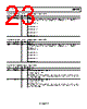
25 / 28 page  Data Sheet ADP1660 Rev. 0 | Page 25 of 28 PCB LAYOUT Poor layout can affect performance, causing electromagnetic interference (EMI) and electromagnetic compatibility (EMC) problems, ground bounce, and power losses. Poor layout can also affect regulation and stability. Figure 32 shows an optimized layout implemented using the following guidelines: • Place the inductor, input capacitor, and output capacitor close to the IC using short tracks. These components carry high switching frequencies and large currents. • Use as wide a trace as possible between the inductor and the SW pin. The easiest path for this trace is through the center of the output capacitor. • Route the LED1/LED2 path away from the inductor and SW node to minimize noise and magnetic interference. • Maximize the size of ground metal on the component side of the board to help with thermal dissipation. • Use a ground plane with two or three vias connecting to the component side ground near the output capacitor to reduce noise interference on sensitive circuit nodes. Analog Devices applications engineers can be contacted through the Analog Devices sales team to discuss different layouts based on system design constraints. LED2 DIGITAL INPUT/ OUTPUT PGND C1 L1 LED1 AREA = 16.4mm2 Li-ION+ INDUCTOR C2 Figure 32. Layout of the ADP1660 Driving a High Power White LED |
|
|
링크 URL |
| ALLDATASHEET 가 귀하에 도움이 되셨나요? [ DONATE ] |
Alldatasheet는? | 광고문의 | 운영자에게 연락하기 | 개인정보취급방침 | 링크 투 데이터시트 | 링크교환 | 제조사별 검색 All Rights Reserved©Alldatasheet.com |
| Russian : Alldatasheetru.com | Korean : Alldatasheet.co.kr | Spanish : Alldatasheet.es | French : Alldatasheet.fr | Italian : Alldatasheetit.com Portuguese : Alldatasheetpt.com | Polish : Alldatasheet.pl | Vietnamese : Alldatasheet.vn Indian : Alldatasheet.in | Mexican : Alldatasheet.com.mx | British : Alldatasheet.co.uk | New Zealand : Alldatasheet.co.nz |
|
Family Site : ic2ic.com |
icmetro.com |
 Korean ▼
 English
 Chinese
 German
 Japanese
 Russian
 Korean
 Spanish
 French
 Italian
 Portuguese
 Polish
 Vietnamese
 Indian
 Mexican
 British
 New Zealand