|
전자부품 데이터시트 검색엔진 |
|
|
전자부품 데이터시트 검색엔진 |
|
ENA2290 데이터시트(PDF) 2 Page - ON Semiconductor |
|
|
|||||||||||||||||||||||||||||
ENA2290 데이터시트(HTML) 2 Page - ON Semiconductor |
|
|
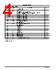
2 / 20 page  STK984-090A-E NoA2290-2/20 Recommended Operating Conditions at Ta = 25 C Parameter Symbol Test Conditions Ratings Unit min. typ. max. Supply Voltage V+B1 +B1 to PG 8 13.5 18 V V+B2 +B2 to SG Output Current Io Io ON Duty, ON Duty100% 120deg Excitation Method - - 20 A Operating Substrate Temperature Tc Thick Film IC Substrate Temperature 40 - 125 C Drive PWM Frequency Fo ONDuty : 10 to 90%,100% - - 20 kHz Thermal Resistance Parameter Symbol Conditions Ratings Unit min. typ. max. Chip-Case Resistance θjc Junction -to- backside of the substrate MOSFET/ch - 4.5 - C /W Electrical Characteristics at Ta = 25 C, V+B1 (V+B2) = 13.5V unless otherwise specifed Parameter Symbol Test Conditions min typ max Unit Current consumption (Control system) ICC V+B1=V+B2=16V 10 15 mA Output saturation voltage VDS(sat) IO=20A +B1 to U, V, W 0.3 0.5 V U, V, W to PG 0.2 0.4 Current sensing resistor Rs 2.91 3.00 3.09 m Time delay (ON) td(on) 20A U, V, W 0.9 1.8 2.8 s U-, V-, W- 0.9 1.9 3.0 Rise time tr 20A 0.3 s Time delay (OFF) td(off) 20A U, V, W 1.3 2.9 4.5 s U-, V-, W- 0.8 2.2 3.5 Fall time tf 20A 0.3 s Motor Control Input Terminal at 8V≤V+B1(V+B2)≤18V, 40C≤Ta≤125C Parameter Symbol Conditions Ratings Unit min. typ. max. Input ON Voltage Vin(on) Output on UT,VT,WT,UB,VB,WB to SG 3.5 - - V Input OFF Voltage Vin(off) Output off UT,VT,WT,UB,VB,WB to SG - - 1.5 V Reset Input Terminal at 8V≤V+B1(V+B2) ≤18V, 40C≤Ta≤125C Parameter Symbol Test Conditions Ratings Unit min. typ. max. Reset High Voltage Vreset(Hi) Output ON 3.5 - - V Reset Low Voltage Vreset(Lo) Output OFF - - 1.5 V Output Delay Time (ON) treset(on) From Reset Input Terminal (RESET=Hi) to Output ON - 0.25 - ms Output Delay Time (OFF) treset(off) From Reset Input Terminal (RESET=Lo) to Output OFF - 2 - s Functional operation above the stresses listed in the Recommended Operating Ranges is not implied. Extended exposure to stresses beyond the Recommended Operating Ranges limits may affect device reliability. Product parametric performance is indicated in the Electrical Characteristics for the listed test conditions, unless otherwise noted. Product performance may not be indicated by the Electrical Characteristics if operated under different conditions. |
|
|
링크 URL |
| ALLDATASHEET 가 귀하에 도움이 되셨나요? [ DONATE ] |
Alldatasheet는? | 광고문의 | 운영자에게 연락하기 | 개인정보취급방침 | 링크 투 데이터시트 | 링크교환 | 제조사별 검색 All Rights Reserved©Alldatasheet.com |
| Russian : Alldatasheetru.com | Korean : Alldatasheet.co.kr | Spanish : Alldatasheet.es | French : Alldatasheet.fr | Italian : Alldatasheetit.com Portuguese : Alldatasheetpt.com | Polish : Alldatasheet.pl | Vietnamese : Alldatasheet.vn Indian : Alldatasheet.in | Mexican : Alldatasheet.com.mx | British : Alldatasheet.co.uk | New Zealand : Alldatasheet.co.nz |
|
Family Site : ic2ic.com |
icmetro.com |
 Korean ▼
 English
 Chinese
 German
 Japanese
 Russian
 Korean
 Spanish
 French
 Italian
 Portuguese
 Polish
 Vietnamese
 Indian
 Mexican
 British
 New Zealand