|
전자부품 데이터시트 검색엔진 |
|
|
전자부품 데이터시트 검색엔진 |
|
TDA3602 데이터시트(PDF) 5 Page - NXP Semiconductors |
|
|
|||||||||||||||||||||||||||||
TDA3602 데이터시트(HTML) 5 Page - NXP Semiconductors |
|
|
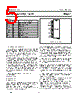
5 / 26 page  July 1994 5 Philips Semiconductors Product specification Multiple output voltage regulator TDA3602 PINNING SYMBOL PIN DESCRIPTION VP 1 positive supply voltage REG1 2 Regulator 1 output RESET 3 reset output Vsc 4 state control input HOLD 5 hold output GND 6 ground REG3 7 Regulator 3 output Vbu 8 back-up REG2 9 Regulator 2 output handbook, halfpage MCD345 1 2 3 4 5 6 7 8 9 P V GND REG1 REG3 REG2 TDA3602 sc V bu V RESET HOLD Fig.2 Pin configuration. FUNCTIONAL DESCRIPTION This multiple output voltage regulator contains three fixed voltage regulators, numbered 1, 2 and 3. Two of these can be switched between the on and off states using the state control pin (pin 4). The third (Regulator 3), which is continuously in, can be switched by the state control pin between a low and a high current mode. In addition to Regulators 1 and 2, the device is supplied by an internal switch that is open when the supply voltage falls below the back-up voltage (negative field decay or engine start procedure), or during a load dump. (During this load dump, Regulators 1 and 2 are switched off and RESET is switched LOW). This switched supply voltage (the so-called back-up voltage (Vbu), is available at pin 8. An electrolytic capacitor can be connected to this pin, and the charge on this capacitor can be used to supply the device for a short period after the supply voltage is removed. Three pins are provided for interfacing with a microprocessor: • state control pin • hold output pin • reset output pin. When the supply voltage (VP) is connected to the device, Vbu will rise. When Vbu reaches 7.9 V, the device is in the power-on mode. The RESET output goes HIGH and Regulator 3 is switched on. In a microprocessor application, the RESET output can be used to call up the CPU and to initialize the program. What follows depends on the voltage at the state control pin (Vsc). In most applications, when the supply voltage is connected, Vsc will rise slowly (e.g. by charging a capacitor).The device will leave the power-on mode and enter the reset mode when Vsc rises above 2.2 V. In both the power-on and reset modes, Regulator 3 will be in the high current mode, Regulators 1 and 2 will be switched off and the RESET output will be HIGH. The device will enter the wake mode when Vsc reaches 2.8 V. The RESET pin will go LOW and the CPU must be switched to the sleep mode. Regulator 3 is still in the high current mode. As Vsc continues rising and the voltage reaches 3.6 V, the stabilizer will be switched into the sleep mode. It will be in a coma mode when Vsc is greater than 3.8 V. In this mode, only the relevant circuits remain operating; this is to keep the power consumption as low as possible i.e. typically 290 µA. If the device is switched on with Vsc already higher than 3.8 V, the device will be switched directly from the power-on mode into the coma mode. When Vsc is lowered gradually from 3.6 V (or higher) to 2 V, the device will go from sleep to reset again. Vsc must be lower than 1.1 V to bring the device into the on mode; note that this is not the same as the power-on mode. In this condition, Regulator 3 is in the high current mode, both Regulators 1 and 2 are switched on and the HOLD output will be HIGH (depending on the state of VP and the in-regulation condition of Regulators 1 and 2). |
|
|
링크 URL |
| ALLDATASHEET 가 귀하에 도움이 되셨나요? [ DONATE ] |
Alldatasheet는? | 광고문의 | 운영자에게 연락하기 | 개인정보취급방침 | 링크 투 데이터시트 | 링크교환 | 제조사별 검색 All Rights Reserved©Alldatasheet.com |
| Russian : Alldatasheetru.com | Korean : Alldatasheet.co.kr | Spanish : Alldatasheet.es | French : Alldatasheet.fr | Italian : Alldatasheetit.com Portuguese : Alldatasheetpt.com | Polish : Alldatasheet.pl | Vietnamese : Alldatasheet.vn Indian : Alldatasheet.in | Mexican : Alldatasheet.com.mx | British : Alldatasheet.co.uk | New Zealand : Alldatasheet.co.nz |
|
Family Site : ic2ic.com |
icmetro.com |
 Korean ▼
 English
 Chinese
 German
 Japanese
 Russian
 Korean
 Spanish
 French
 Italian
 Portuguese
 Polish
 Vietnamese
 Indian
 Mexican
 British
 New Zealand