|
전자부품 데이터시트 검색엔진 |
|
|
전자부품 데이터시트 검색엔진 |
|
TDA3602 데이터시트(PDF) 20 Page - NXP Semiconductors |
|
|
|||||||||||||||||||||||||||||
TDA3602 데이터시트(HTML) 20 Page - NXP Semiconductors |
|
|
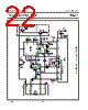
20 / 26 page  July 1994 20 Philips Semiconductors Product specification Multiple output voltage regulator TDA3602 The timing diagram can only be understood after a thorough investigation of the flow charts (see section Flow chart semi on/off logic with security code). Furthermore short and long RESET pulses can be seen (see Fig.12). Flowchart semi on/off logic with security code This section describes the software for controlling the TDA3602 (semi on/off logic). A “o” in the flowchart flow diagram Fig.13, indicates that the port mentioned is switched as an output. A “1” indicates that the port mentioned is switched as an input (temporarily). The flowchart of figure 13 can be used for semi on/off logic. handbook, full pagewidth MSA724 V battery A4 ignition A7 VREG3 reset microprocessor reset VSC S1 microprocessor REGULATORS 1 and 2 hold P0. 0 initialization on switch 1 off on engine start load dump off by ignition Fig.12 Timing of the applications. |
|
|
링크 URL |
| ALLDATASHEET 가 귀하에 도움이 되셨나요? [ DONATE ] |
Alldatasheet는? | 광고문의 | 운영자에게 연락하기 | 개인정보취급방침 | 링크 투 데이터시트 | 링크교환 | 제조사별 검색 All Rights Reserved©Alldatasheet.com |
| Russian : Alldatasheetru.com | Korean : Alldatasheet.co.kr | Spanish : Alldatasheet.es | French : Alldatasheet.fr | Italian : Alldatasheetit.com Portuguese : Alldatasheetpt.com | Polish : Alldatasheet.pl | Vietnamese : Alldatasheet.vn Indian : Alldatasheet.in | Mexican : Alldatasheet.com.mx | British : Alldatasheet.co.uk | New Zealand : Alldatasheet.co.nz |
|
Family Site : ic2ic.com |
icmetro.com |
 Korean ▼
 English
 Chinese
 German
 Japanese
 Russian
 Korean
 Spanish
 French
 Italian
 Portuguese
 Polish
 Vietnamese
 Indian
 Mexican
 British
 New Zealand