|
전자부품 데이터시트 검색엔진 |
|
|
전자부품 데이터시트 검색엔진 |
|
TDA3602 데이터시트(PDF) 23 Page - NXP Semiconductors |
|
|
|||||||||||||||||||||||||||||
TDA3602 데이터시트(HTML) 23 Page - NXP Semiconductors |
|
|
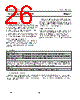
23 / 26 page  July 1994 23 Philips Semiconductors Product specification Multiple output voltage regulator TDA3602 halfpage MSA727 START P1, 1 = 1 (i) X = Sx X Sx + 4 ? no yes P0, X = 0 Y = Sy Y Sy + 4 ? no input P1, Y Y = Y + 1 yes P0, X = 1 X = X + 1 P1, 1 = 0 (o) STOP t R4 x C6 x in (5/3) t 2.4 ms Fig.15 Software key matrix with loops. FULL ON/OFF LOGIC Using application circuit Fig.14, full on/off logic can be achieved. Also extra software loops are required to enable the set when ignition is off. The set can be controlled by Port P1,1 if the ignition is off (thus no extra I/O ports of the microprocessor are required for full on/off logic). Because Port P1,1 is a part of the key matrix the complete key-scan loop must be finished within less than 0.5 × R4 × C6 = 2.4 ms, otherwise the TDA3602 will enter the reset state and Regulators 1 and 2 are switched off during this key-scan loop. When the time of the complete loop is within 2.4 ms the Vsc will remain below 2 V (thus Regulators 1 and 2 remain on). It is also possible to switch Port P1,1 during the key-scan loop sequentially from output (logic 0) to input. If this is achieved within a time period of 1 ms, Vsc cannot become HIGH long enough to switch Regulators 1 and 2 off. When ignition is available, transistor T1 overrules Port P1,1. In this event no variation on Vsc is seen during the key-scan loop. The flow chart presented in Fig.15 is only required for the full on/off logic application of Fig.14. The complete key-scan routine must be finished within 2.4 ms (when ignition is off) and that the key-scan routine has to end with a statement P1,1 = logic 0. In the flow chart of the key-scan routine, Sx is the start value of the rows and Sy the start value of the columns. With Sx = 1 and Sy = 1, one '0' is shifted on the output ports P0,1 to P0,5 and the input ports P1,1 to P1,5 are being read sequentially per shift action. Connections between microprocessor and Regulator 2 supplied When digital ICs, supplied by Regulator 2, are connected to I/O ports (especially Ports 1 and 2), special attention in the software has to be taken to avoid currents flowing from Regulator 3 to Regulator 2. Because of ESD diodes in digital ICs a current can flow from an output port (which is in a high state) through the ESD diode into Regulator 2. This will cause an increase in the quiescent current of the set. The recommended action to avoid this problem is to switch the specific I/O ports to logic 0. |
|
|
링크 URL |
| ALLDATASHEET 가 귀하에 도움이 되셨나요? [ DONATE ] |
Alldatasheet는? | 광고문의 | 운영자에게 연락하기 | 개인정보취급방침 | 링크 투 데이터시트 | 링크교환 | 제조사별 검색 All Rights Reserved©Alldatasheet.com |
| Russian : Alldatasheetru.com | Korean : Alldatasheet.co.kr | Spanish : Alldatasheet.es | French : Alldatasheet.fr | Italian : Alldatasheetit.com Portuguese : Alldatasheetpt.com | Polish : Alldatasheet.pl | Vietnamese : Alldatasheet.vn Indian : Alldatasheet.in | Mexican : Alldatasheet.com.mx | British : Alldatasheet.co.uk | New Zealand : Alldatasheet.co.nz |
|
Family Site : ic2ic.com |
icmetro.com |
 Korean ▼
 English
 Chinese
 German
 Japanese
 Russian
 Korean
 Spanish
 French
 Italian
 Portuguese
 Polish
 Vietnamese
 Indian
 Mexican
 British
 New Zealand