|
전자부품 데이터시트 검색엔진 |
|
|
전자부품 데이터시트 검색엔진 |
|
ADAR4002ACPZ-R7 데이터시트(PDF) 11 Page - Analog Devices |
|
|
|||||||||||||||||||||||||||||
ADAR4002ACPZ-R7 데이터시트(HTML) 11 Page - Analog Devices |
|
|
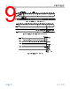
11 / 66 page  Data Sheet ADAR4002 SPECIFICATIONS analog.com Rev. A | 11 of 66 SHIFT REGISTER MODE The ADAR4002 offers an extremely simple serial shift register mode by asserting the MODE pin high. In this mode, there are no register addresses, no sequencer functionality, and no short commands. The shift register has dual rank data registers and is controlled with the UPDATE pin. The digital pins of the ADAR4002 are configured for a daisy-chain operation, with the possibility of one ADAR4002 driving another, in as long a chain as required. Data comes in on CLK_IN and DATA_IO and shifts out on CSB/CLKO and DATA_O. Data is serially shifted through the full chain of the devices. Once the correct TDU and DSA data are in the correct devices, an update signal is given to load the data into the second rank register of the several devices. The second rank register data is immediately applied to the various TDUs and DSAs on all the daisy chained ADAR4002 devices. Shift register mode timing is shown in Figure 8. Figure 8. Timing Diagram for Two ADAR4002 Chips Daisy-Chained Together While in Shift Register Mode (Chip 1 Drives Chip 2) |
|
링크 URL |
| ALLDATASHEET 가 귀하에 도움이 되셨나요? [ DONATE ] |
Alldatasheet는? | 광고문의 | 운영자에게 연락하기 | 개인정보취급방침 | 링크 투 데이터시트 | 링크교환 | 제조사별 검색 All Rights Reserved©Alldatasheet.com |
| Russian : Alldatasheetru.com | Korean : Alldatasheet.co.kr | Spanish : Alldatasheet.es | French : Alldatasheet.fr | Italian : Alldatasheetit.com Portuguese : Alldatasheetpt.com | Polish : Alldatasheet.pl | Vietnamese : Alldatasheet.vn Indian : Alldatasheet.in | Mexican : Alldatasheet.com.mx | British : Alldatasheet.co.uk | New Zealand : Alldatasheet.co.nz |
|
Family Site : ic2ic.com |
icmetro.com |
 Korean ▼
 English
 Chinese
 German
 Japanese
 Russian
 Korean
 Spanish
 French
 Italian
 Portuguese
 Polish
 Vietnamese
 Indian
 Mexican
 British
 New Zealand