|
전자부품 데이터시트 검색엔진 |
|
|
전자부품 데이터시트 검색엔진 |
|
ADAR4002ACPZ-R7 데이터시트(PDF) 13 Page - Analog Devices |
|
|
|||||||||||||||||||||||||||||
ADAR4002ACPZ-R7 데이터시트(HTML) 13 Page - Analog Devices |
|
|
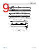
13 / 66 page  Data Sheet ADAR4002 PIN CONFIGURATION AND FUNCTION DESCRIPTIONS analog.com Rev. A | 13 of 66 Figure 9. ADAR4002 Pin Configuration Table 8. Pin Function Descriptions Pin No. Mnemonic Description 1, 3, 8, 10 GND RF and Analog Ground. Tie all ground pads together to a low impedance plane on the circuit board. 2 RF1 RF Input or Output Looking into the DSA. Internal DC bias is 0 V. AC coupling is required if the bias of the connected device differs so that the ADAR4002 internal bias is not disturbed. 4 V1P0 Digital Supply. Apply 1.0 V. 5 CLK_IN Serial Clock Input for Both Digital Modes (1.0 V Logic). 6 DATA_IO Dual Direction Pin. DATA_IO is used for both SPI mode and shift register mode. While in the 3-wire SPI protocol, this pin is the serial data input and output. While in the 4-wire SPI protocol, this pin is the serial data input. While in shift register mode, this pin is the register data input (1.0 V logic). 7 MODE Digital Mode Select for Digital Input and Output Data (1.0 V Logic). If MODE is low (ground), it is in SPI mode, and if MODE is high, it is in shift register mode. 9 RF2 RF Input or Output Looking into the TDU. Internal DC bias is 0 V. AC coupling is required if the bias of the connected device differs so that the ADAR4002 internal bias is not disturbed. 11 V1P2 RF Supply Voltage. Apply 1.2 V. 12 DATA_O Serial Data Output for Both Digital Modes. While in the 4-wire SPI protocol, this pin is the serial data output. While in shift register mode, this pin is the shift register data output (1.0 V logic). 13 CSB/CLKO While in SPI mode, chip select (CSB). While in shift register mode, clock output (1.0 V logic). 14 UPDATE While in SPI mode, UPDATE advances the sequencer. While in shift register mode, UPDATE loads data from the shift register to TDU and DSA (1.0 V logic). EP Exposed Pad RF and Analog Ground. Tie to a low impedance ground plane on the PCB. |
|
링크 URL |
| ALLDATASHEET 가 귀하에 도움이 되셨나요? [ DONATE ] |
Alldatasheet는? | 광고문의 | 운영자에게 연락하기 | 개인정보취급방침 | 링크 투 데이터시트 | 링크교환 | 제조사별 검색 All Rights Reserved©Alldatasheet.com |
| Russian : Alldatasheetru.com | Korean : Alldatasheet.co.kr | Spanish : Alldatasheet.es | French : Alldatasheet.fr | Italian : Alldatasheetit.com Portuguese : Alldatasheetpt.com | Polish : Alldatasheet.pl | Vietnamese : Alldatasheet.vn Indian : Alldatasheet.in | Mexican : Alldatasheet.com.mx | British : Alldatasheet.co.uk | New Zealand : Alldatasheet.co.nz |
|
Family Site : ic2ic.com |
icmetro.com |
 Korean ▼
 English
 Chinese
 German
 Japanese
 Russian
 Korean
 Spanish
 French
 Italian
 Portuguese
 Polish
 Vietnamese
 Indian
 Mexican
 British
 New Zealand