|
전자부품 데이터시트 검색엔진 |
|
|
전자부품 데이터시트 검색엔진 |
|
AT45DB021D 데이터시트(PDF) 10 Page - ATMEL Corporation |
|
|
|||||||||||||||||||||||||||||
AT45DB021D 데이터시트(HTML) 10 Page - ATMEL Corporation |
|
|
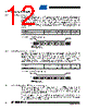
10 / 52 page  10 3638F–DFLASH–4/08 AT45DB021D 7.7 Chip Erase The entire main memory can be erased at one time by using the Chip Erase command. To execute the Chip Erase command, a 4-byte command sequence C7H, 94H, 80H and 9AH must be clocked into the device. Since the entire memory array is to be erased, no address bytes need to be clocked into the device, and any data clocked in after the opcode will be ignored. After the last bit of the opcode sequence has been clocked in, the CS pin can be deas- serted to start the erase process. The erase operation is internally self-timed and should take place in a time of t CE. During this time, the Status Register will indicate that the device is busy. The Chip Erase command will not affect sectors that are protected or locked down; the contents of those sectors will remain unchanged. Only those sectors that are not protected or locked down will be erased. The WP pin can be asserted while the device is erasing, but protection will not be activated until the internal erase cycle completes. Figure 7-1. Chip Erase Table 7-2. Sector Erase Addressing PA9/ A17 PA8/ A16 PA7/ A15 PA6/ A14 PA5/ A13 PA4/ A12 PA3/ A11 PA2/ A10 PA1/ A9 PA0/ A8 Sector 0000000 X X X 0a 0000001 X X X 0b • • • • • • • • • • • • • • • • • • • • • • • • • • • • • • • • • 0 1 1 XXXXX XX 5 1 0 0 XXXXX XX 6 1 1 1 XXXXX XX 7 Command Byte 1 Byte 2 Byte 3 Byte 4 Chip Erase C7H 94H 80H 9AH Opcode Byte 1 Opcode Byte 2 Opcode Byte 3 Opcode Byte 4 CS Each transition represents 8 bits SI |
|
링크 URL |
| ALLDATASHEET 가 귀하에 도움이 되셨나요? [ DONATE ] |
Alldatasheet는? | 광고문의 | 운영자에게 연락하기 | 개인정보취급방침 | 링크 투 데이터시트 | 링크교환 | 제조사별 검색 All Rights Reserved©Alldatasheet.com |
| Russian : Alldatasheetru.com | Korean : Alldatasheet.co.kr | Spanish : Alldatasheet.es | French : Alldatasheet.fr | Italian : Alldatasheetit.com Portuguese : Alldatasheetpt.com | Polish : Alldatasheet.pl | Vietnamese : Alldatasheet.vn Indian : Alldatasheet.in | Mexican : Alldatasheet.com.mx | British : Alldatasheet.co.uk | New Zealand : Alldatasheet.co.nz |
|
Family Site : ic2ic.com |
icmetro.com |
 Korean ▼
 English
 Chinese
 German
 Japanese
 Russian
 Korean
 Spanish
 French
 Italian
 Portuguese
 Polish
 Vietnamese
 Indian
 Mexican
 British
 New Zealand