|
전자부품 데이터시트 검색엔진 |
|
|
전자부품 데이터시트 검색엔진 |
|
AT45DB021D 데이터시트(PDF) 4 Page - ATMEL Corporation |
|
|
|||||||||||||||||||||||||||||
AT45DB021D 데이터시트(HTML) 4 Page - ATMEL Corporation |
|
|
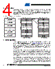
4 / 52 page  4 3638F–DFLASH–4/08 AT45DB021D 4. Memory Array To provide optimal flexibility, the memory array of the AT45DB021D is divided into three levels of granularity comprising of sectors, blocks, and pages. The “Memory Architecture Diagram” illus- trates the breakdown of each level and details the number of pages per sector and block. All program operations to the DataFlash occur on a page-by-page basis. The erase operations can be performed at the chip, sector, block or page level. Figure 4-1. Memory Architecture Diagram 5. Device Operation The device operation is controlled by instructions from the host processor. The list of instructions and their associated opcodes are contained in Tables 15-1 through 15-7. A valid instruction starts with the falling edge of CS followed by the appropriate 8-bit opcode and the desired buffer or main memory address location. While the CS pin is low, toggling the SCK pin controls the loading of the opcode and the desired buffer or main memory address location through the SI (serial input) pin. All instructions, addresses, and data are transferred with the most significant bit (MSB) first. Buffer addressing for the DataFlash standard page size (264 bytes) is referenced in the datasheet using the terminology BFA8 - BFA0 to denote the 9 address bits required to designate a byte address within a buffer. Main memory addressing is referenced using the terminology PA9 - PA0 and BA8 - BA0, where PA9 - PA0 denotes the 10 address bits required to designate a page address and BA8 - BA0 denotes the 9 address bits required to designate a byte address within the page. For the “Power of 2” binary page size (256 bytes), the Buffer addressing is referenced in the datasheet using the conventional terminology BFA7 - BFA0 to denote the 8 address bits required to designate a byte address within a buffer. Main memory addressing is referenced using the terminology A17 - A0, where A17 - A8 denotes the 10 address bits required to desig- nate a page address and A7 - A0 denotes the 8 address bits required to designate a byte address within a page. SECTOR 0a = 8 Pages 2,048/2,112 bytes SECTOR 0b = 120 Pages 31,744/32,726 bytes Block = 1,024/1,056 bytes 8 Pages SECTOR 0a Page = 256/264 bytes PAGE 0 PAGE 1 PAGE 6 PAGE 7 PAGE 8 PAGE 9 PAGE 1,022 PAGE 1,023 PAGE 14 PAGE 15 PAGE 16 PAGE 17 PAGE 18 SECTOR ARCHITECTURE BLOCK ARCHITECTURE PAGE ARCHITECTURE BLOCK 0 BLOCK 1 BLOCK 14 BLOCK 15 BLOCK 16 BLOCK 17 BLOCK 126 BLOCK 127 BLOCK 30 BLOCK 31 BLOCK 32 BLOCK 33 SECTOR 7 = 128 Pages 32,768/33,792 bytes BLOCK 2 SECTOR 1 = 128 Pages 32,768/33,792 bytes SECTOR 6 = 128 Pages 32,768/33,792 bytes |
|
링크 URL |
| ALLDATASHEET 가 귀하에 도움이 되셨나요? [ DONATE ] |
Alldatasheet는? | 광고문의 | 운영자에게 연락하기 | 개인정보취급방침 | 링크 투 데이터시트 | 링크교환 | 제조사별 검색 All Rights Reserved©Alldatasheet.com |
| Russian : Alldatasheetru.com | Korean : Alldatasheet.co.kr | Spanish : Alldatasheet.es | French : Alldatasheet.fr | Italian : Alldatasheetit.com Portuguese : Alldatasheetpt.com | Polish : Alldatasheet.pl | Vietnamese : Alldatasheet.vn Indian : Alldatasheet.in | Mexican : Alldatasheet.com.mx | British : Alldatasheet.co.uk | New Zealand : Alldatasheet.co.nz |
|
Family Site : ic2ic.com |
icmetro.com |
 Korean ▼
 English
 Chinese
 German
 Japanese
 Russian
 Korean
 Spanish
 French
 Italian
 Portuguese
 Polish
 Vietnamese
 Indian
 Mexican
 British
 New Zealand