|
전자부품 데이터시트 검색엔진 |
|
|
전자부품 데이터시트 검색엔진 |
|
TMP86CS49FG 데이터시트(PDF) 66 Page - Toshiba Semiconductor |
|
|
|||||||||||||||||||||||||||||
TMP86CS49FG 데이터시트(HTML) 66 Page - Toshiba Semiconductor |
|
|
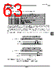
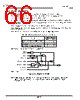
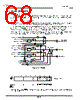
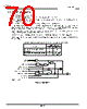
66 / 252 page  Page 52 5. I/O Ports 5.2 Port P1 (P17 to P10) TMP86CS49FG 5.2 Port P1 (P17 to P10) Port P1 is an 8-bit input/output port which can be configured as an input or output in one-bit unit. Port P1 is also used as a timer/counter input/output, an external interrupt input and a divider output. Input/output mode is specified by the P1 control register (P1CR). During reset, the P1CR is initialized to "0" and port P1 becomes an input mode. And the P1DR is initialized to "0". When used as an input port, a timer/counter input and an external interrupt input, the corresponding bit of P1CR should be set to "0". When used as an output port, the corresponding bit of P1CR should be set to "1". When used as a timer/counter output and a divider output, P1DR is set to "1" beforehand and the corresponding bit of P1CR should be set to "1". When P1CR is "1", the content of the corresponding output latch is read by reading P1DR. Note: Asterisk (*) indicates “1” or “0” either of which can be selected. Note: i = 7 to 0 Figure 5-3 Port 1 and P1CR Note: The port set to an input mode reads the terminal input data. Therefore, when the input and output modes are used together, the content of the output latch which is specified as input mode might be changed by executing a bit Manipulation instruction. Table 5-2 Register Programming for Multi-function Ports Function Programmed Value P1DR P1CR Port input, timer/counter input or external interrupt input *“0” Port “0” output “0” “1” Port “1” output, a timer output or a divider output “1” “1” P1i DQ DQ STOP OUTEN P1CRi P1CRi input Data input (P1DR) Data output (P1DR) Control output Control input Output latch |
|
링크 URL |
| ALLDATASHEET 가 귀하에 도움이 되셨나요? [ DONATE ] |
Alldatasheet는? | 광고문의 | 운영자에게 연락하기 | 개인정보취급방침 | 링크 투 데이터시트 | 링크교환 | 제조사별 검색 All Rights Reserved©Alldatasheet.com |
| Russian : Alldatasheetru.com | Korean : Alldatasheet.co.kr | Spanish : Alldatasheet.es | French : Alldatasheet.fr | Italian : Alldatasheetit.com Portuguese : Alldatasheetpt.com | Polish : Alldatasheet.pl | Vietnamese : Alldatasheet.vn Indian : Alldatasheet.in | Mexican : Alldatasheet.com.mx | British : Alldatasheet.co.uk | New Zealand : Alldatasheet.co.nz |
|
Family Site : ic2ic.com |
icmetro.com |
 Korean ▼
 English
 Chinese
 German
 Japanese
 Russian
 Korean
 Spanish
 French
 Italian
 Portuguese
 Polish
 Vietnamese
 Indian
 Mexican
 British
 New Zealand