|
전자부품 데이터시트 검색엔진 |
|
|
전자부품 데이터시트 검색엔진 |
|
TMP86CS49FG 데이터시트(PDF) 31 Page - Toshiba Semiconductor |
|
|
|||||||||||||||||||||||||||||
TMP86CS49FG 데이터시트(HTML) 31 Page - Toshiba Semiconductor |
|
|
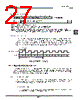
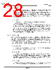
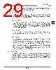
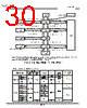
31 / 252 page  Page 17 TMP86CS49FG Note 1: Always set RETM to “0” when transiting from NORMAL mode to STOP mode. Always set RETM to “1” when transiting from SLOW mode to STOP mode. Note 2: When STOP mode is released with RESET pin input, a return is made to NORMAL1 regardless of the RETM contents. Note 3: fc: High-frequency clock [Hz], fs: Low-frequency clock [Hz], *; Don’t care Note 4: Bits 1 and 0 in SYSCR1 are read as undefined data when a read instruction is executed. Note 5: As the hardware becomes STOP mode under OUTEN = “0”, input value is fixed to “0”; therefore it may cause external interrupt request on account of falling edge. Note 6: When the key-on wakeup is used, RELM should be set to "1". Note 7: Port P20 is used as STOP pin. Therefore, when stop mode is started, OUTEN does not affect to P20, and P20 becomes High-Z mode. Note 8: The warmig-up time should be set correctly for using oscillator. Note 1: A reset is applied if both XEN and XTEN are cleared to “0”, XEN is cleared to “0” when SYSCK = “0”, or XTEN is cleared to “0” when SYSCK = “1”. Note 2: *: Don’t care, TG: Timing generator, *; Don’t care Note 3: Bits 3, 1 and 0 in SYSCR2 are always read as undefined value. Note 4: Do not set IDLE and TGHALT to “1” simultaneously. Note 5: Because returning from IDLE0/SLEEP0 to NORMAL1/SLOW1 is executed by the asynchronous internal clock, the period of IDLE0/SLEEP0 mode might be shorter than the period setting by TBTCR<TBTCK>. Note 6: When IDLE1/2 or SLEEP1/2 mode is released, IDLE is automatically cleared to “0”. Note 7: When IDLE0 or SLEEP0 mode is released, TGHALT is automatically cleared to “0”. Note 8: Before setting TGHALT to “1”, be sure to stop peripherals. If peripherals are not stopped, the interrupt latch of peripherals may be set after IDLE0 or SLEEP0 mode is released. System Control Register 1 SYSCR1 76 543 21 0 (0038H) STOP RELM RETM OUTEN WUT (Initial value: 0000 00**) STOP STOP mode start 0: CPU core and peripherals remain active 1: CPU core and peripherals are halted (Start STOP mode) R/W RELM Release method for STOP mode 0: Edge-sensitive release 1: Level-sensitive release R/W RETM Operating mode after STOP mode 0: Return to NORMAL1/2 mode 1: Return to SLOW1 mode R/W OUTEN Port output during STOP mode 0: High impedance 1: Output kept R/W WUT Warm-up time at releasing STOP mode Return to NORMAL mode Return to SLOW mode R/W 00 01 10 11 3 x 216/fc 216/fc 3 x 214/fc 214/fc 3 x 213/fs 213/fs 3 x 26/fs 26/fs System Control Register 2 SYSCR2 (0039H) 76 543 21 0 XEN XTEN SYSCK IDLE TGHALT (Initial value: 1000 *0**) XEN High-frequency oscillator control 0: Turn off oscillation 1: Turn on oscillation R/W XTEN Low-frequency oscillator control 0: Turn off oscillation 1: Turn on oscillation SYSCK Main system clock select (Write)/main system clock moni- tor (Read) 0: High-frequency clock (NORMAL1/NORMAL2/IDLE1/IDLE2) 1: Low-frequency clock (SLOW1/SLOW2/SLEEP1/SLEEP2) IDLE CPU and watchdog timer control (IDLE1/2 and SLEEP1/2 modes) 0: CPU and watchdog timer remain active 1: CPU and watchdog timer are stopped (Start IDLE1/2 and SLEEP1/2 modes) R/W TGHALT TG control (IDLE0 and SLEEP0 modes) 0: Feeding clock to all peripherals from TG 1: Stop feeding clock to peripherals except TBT from TG. (Start IDLE0 and SLEEP0 modes) |
|
링크 URL |
| ALLDATASHEET 가 귀하에 도움이 되셨나요? [ DONATE ] |
Alldatasheet는? | 광고문의 | 운영자에게 연락하기 | 개인정보취급방침 | 링크 투 데이터시트 | 링크교환 | 제조사별 검색 All Rights Reserved©Alldatasheet.com |
| Russian : Alldatasheetru.com | Korean : Alldatasheet.co.kr | Spanish : Alldatasheet.es | French : Alldatasheet.fr | Italian : Alldatasheetit.com Portuguese : Alldatasheetpt.com | Polish : Alldatasheet.pl | Vietnamese : Alldatasheet.vn Indian : Alldatasheet.in | Mexican : Alldatasheet.com.mx | British : Alldatasheet.co.uk | New Zealand : Alldatasheet.co.nz |
|
Family Site : ic2ic.com |
icmetro.com |
 Korean ▼
 English
 Chinese
 German
 Japanese
 Russian
 Korean
 Spanish
 French
 Italian
 Portuguese
 Polish
 Vietnamese
 Indian
 Mexican
 British
 New Zealand