|
전자부품 데이터시트 검색엔진 |
|
|
전자부품 데이터시트 검색엔진 |
|
TMP86CS49FG 데이터시트(PDF) 173 Page - Toshiba Semiconductor |
|
|
|||||||||||||||||||||||||||||
TMP86CS49FG 데이터시트(HTML) 173 Page - Toshiba Semiconductor |
|
|
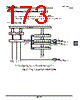
173 / 252 page  Page 159 TMP86CS49FG 14. Synchronous Serial Interface (SIO1) The serial interfaces connect to an external device via SI1, SO1, and SCK1 pins. When these pins are used as serial interface, the output latches for each port should be set to "1". 14.1 Configuration Figure 14-1 Synchronous Serial Interface (SIO) interrupt Internal clock input To BUS Shift register on transmitter Shift register on receiver (Serial data output) Control circuit Shift clock Internal data bus Port (Note) (Serial data output) Port (Note) (Serial data input) Port (Note) Note: Set the register of port correctly for the port assigned as serial interface pins. For details, see the description of the input/output port control register. MSB/LSB selection SO1 pin SI1 pin SIO1TDB SIO1RDB SCK1 pin INTSIO1 SIO1CR SIO1SR |
|
링크 URL |
| ALLDATASHEET 가 귀하에 도움이 되셨나요? [ DONATE ] |
Alldatasheet는? | 광고문의 | 운영자에게 연락하기 | 개인정보취급방침 | 링크 투 데이터시트 | 링크교환 | 제조사별 검색 All Rights Reserved©Alldatasheet.com |
| Russian : Alldatasheetru.com | Korean : Alldatasheet.co.kr | Spanish : Alldatasheet.es | French : Alldatasheet.fr | Italian : Alldatasheetit.com Portuguese : Alldatasheetpt.com | Polish : Alldatasheet.pl | Vietnamese : Alldatasheet.vn Indian : Alldatasheet.in | Mexican : Alldatasheet.com.mx | British : Alldatasheet.co.uk | New Zealand : Alldatasheet.co.nz |
|
Family Site : ic2ic.com |
icmetro.com |
 Korean ▼
 English
 Chinese
 German
 Japanese
 Russian
 Korean
 Spanish
 French
 Italian
 Portuguese
 Polish
 Vietnamese
 Indian
 Mexican
 British
 New Zealand