|
전자부품 데이터시트 검색엔진 |
|
|
전자부품 데이터시트 검색엔진 |
|
TMP86CS49FG 데이터시트(PDF) 233 Page - Toshiba Semiconductor |
|
|
|||||||||||||||||||||||||||||
TMP86CS49FG 데이터시트(HTML) 233 Page - Toshiba Semiconductor |
|
|
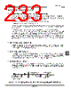
233 / 252 page  Page 219 TMP86CS49FG 17.6 Precautions about AD Converter 17.6.1 Restrictions for AD Conversion interrupt (INTADC) usage When an AD interrupt is used, it may not be processed depending on program composition. For example, if an INTADC interrupt request is generated while an interrupt with priority lower than the interrupt latch IL15 (INTADC) is being accepted, the INTADC interrupt latch may be cleared without the INTADC interrupt being processed. The completion of AD conversion can be detected by the following methods: (1) Method not using the AD conversion end interrupt Whether or not AD conversion is completed can be detected by monitoring the AD conversion end flag (EOCF) by software. This can be done by polling EOCF or monitoring EOCF at regular intervals after start of AD conversion. (2) Method for detecting AD conversion end while a lower-priority interrupt is being processed While an interrupt with priority lower than INTADC is being processed, check the AD conversion end flag (EOCF) and interrupt latch IL15. If IL15 = 0 and EOCF = 1, call the AD conversion end interrupt processing routine with consideration given to PUSH/POP operations. At this time, if an interrupt request with priority higher than INTADC has been set, the AD conversion end interrupt processing routine will be executed first against the specified priority. If necessary, we recommend that the AD conversion end interrupt processing rou- tine be called after checking whether or not an interrupt request with priority higher than INTADC has been set. 17.6.2 Analog input pin voltage range Make sure the analog input pins (AIN0 to AIN15) are used at voltages within VAREF to VSS. If any voltage outside this range is applied to one of the analog input pins, the converted value on that pin becomes uncertain. The other analog input pins also are affected by that. 17.6.3 Analog input shared pins The analog input pins (AIN0 to AIN15) are shared with input/output ports. When using any of the analog inputs to execute AD conversion, do not execute input/output instructions for all other ports. This is necessary to prevent the accuracy of AD conversion from degrading. Not only these analog input shared pins, some other pins may also be affected by noise arising from input/output to and from adjacent pins. 17.6.4 Noise Countermeasure The internal equivalent circuit of the analog input pins is shown in Figure 17-5. The higher the output impedance of the analog input source, more easily they are susceptible to noise. Therefore, make sure the out- put impedance of the signal source in your design is 5 k Ω or less. Toshiba also recommends attaching a capac- itor external to the chip. Figure 17-5 Analog Input Equivalent Circuit and Example of Input Pin Processing DA converter AINi Analog comparator Internal resistance Permissible signal source impedance Internal capacitance 5 k Ω (typ) C = 12 pF (typ.) 5 k Ω (max) Note) i = 15 to 0 |
|
링크 URL |
| ALLDATASHEET 가 귀하에 도움이 되셨나요? [ DONATE ] |
Alldatasheet는? | 광고문의 | 운영자에게 연락하기 | 개인정보취급방침 | 링크 투 데이터시트 | 링크교환 | 제조사별 검색 All Rights Reserved©Alldatasheet.com |
| Russian : Alldatasheetru.com | Korean : Alldatasheet.co.kr | Spanish : Alldatasheet.es | French : Alldatasheet.fr | Italian : Alldatasheetit.com Portuguese : Alldatasheetpt.com | Polish : Alldatasheet.pl | Vietnamese : Alldatasheet.vn Indian : Alldatasheet.in | Mexican : Alldatasheet.com.mx | British : Alldatasheet.co.uk | New Zealand : Alldatasheet.co.nz |
|
Family Site : ic2ic.com |
icmetro.com |
 Korean ▼
 English
 Chinese
 German
 Japanese
 Russian
 Korean
 Spanish
 French
 Italian
 Portuguese
 Polish
 Vietnamese
 Indian
 Mexican
 British
 New Zealand