|
전자부품 데이터시트 검색엔진 |
|
|
전자부품 데이터시트 검색엔진 |
|
LE25LB642CT 데이터시트(PDF) 7 Page - Sanyo Semicon Device |
|
|
|||||||||||||||||||||||||||||
LE25LB642CT 데이터시트(HTML) 7 Page - Sanyo Semicon Device |
|
|
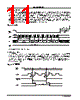
7 / 14 page  LE25LB642CT Description of Commands and Their Operations “Table 1 Command Settings” provides a list and overview of the commands. A detailed description of the functions and operations corresponding to each command is presented below. 1. Read (READ) Consisting of the first through third bus cycles, the read command inputs the 16-bit addresses following (03h), and the data in the designated addresses is output synchronized to SCK. The data is output from SO on the falling edge of third bus cycle bit0 as a reference. “Figure 4 READ” shows the timing waveforms. When SCK is input continuously after the read command has been input and the data in the designated addresses has been output, the address is automatically incremented inside the device while SCK is being input, and the corresponding data is output in sequence. If the SCK input is continued after the internal address arrives at the highest address, the internal address returns to the lowest address (0000h), and data output is continued. By setting the logic level of CS to high, the device is deselected, and the read cycle ends. While the device is deselected, the output pin SO is in a high-impedance state. Figure 4 READ CS SCK SI SO Mode3 High Impedance 8CLK Mode0 0 1 2 3 4 5 6 7 8 15 16 Add. (00000011) Add. 23 24 25 26 27 28 29 30 31 7 654 Data Out(N) Data Out(N+1) 32 10 7 03h (A15-A8) (A7-A0) • Addresses A15 - A13 are “don’t care.” • In synchronization with the rising edges of 0 to 23 clock signals, the command is identified and the addresses are taken in through SI. • In synchronization with the falling edges of 23 clock signal or later, the data is output to SO. No.NA1471-7/14 |
|
|
링크 URL |
| ALLDATASHEET 가 귀하에 도움이 되셨나요? [ DONATE ] |
Alldatasheet는? | 광고문의 | 운영자에게 연락하기 | 개인정보취급방침 | 링크 투 데이터시트 | 링크교환 | 제조사별 검색 All Rights Reserved©Alldatasheet.com |
| Russian : Alldatasheetru.com | Korean : Alldatasheet.co.kr | Spanish : Alldatasheet.es | French : Alldatasheet.fr | Italian : Alldatasheetit.com Portuguese : Alldatasheetpt.com | Polish : Alldatasheet.pl | Vietnamese : Alldatasheet.vn Indian : Alldatasheet.in | Mexican : Alldatasheet.com.mx | British : Alldatasheet.co.uk | New Zealand : Alldatasheet.co.nz |
|
Family Site : ic2ic.com |
icmetro.com |
 Korean ▼
 English
 Chinese
 German
 Japanese
 Russian
 Korean
 Spanish
 French
 Italian
 Portuguese
 Polish
 Vietnamese
 Indian
 Mexican
 British
 New Zealand