|
전자부품 데이터시트 검색엔진 |
|
|
전자부품 데이터시트 검색엔진 |
|
LE25LB642CT 데이터시트(PDF) 8 Page - Sanyo Semicon Device |
|
|
|||||||||||||||||||||||||||||
LE25LB642CT 데이터시트(HTML) 8 Page - Sanyo Semicon Device |
|
|
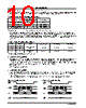
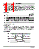
8 / 14 page  LE25LB642CT 2. Status Registers The status registers read the operating and setting statuses inside the device from outside (status register read) and set the protect information (status register write). There are 8 bits in total, and “Table 2 Status Registers” gives the significance of each bit. Table 2 Status Registers Bit Name Logic Function Power-on time Information 0 Ready Bit0 RDY 1 Busy (in write operation) 0 0 Write disabled Bit1 WEN 1 Write enabled 0 0 Bit2 BP0 1 Nonvolatile information 0 Bit3 BP1 1 Block protect information See status register description on BP0 and BP1 Nonvolatile information Bit4 × 0 Reserved bit 0 Bit5 × 0 Reserved bit 0 Bit6 × 0 Reserved bit 0 0 Status register write enabled Bit7 SRWP 1 Status register write disabled Nonvolatile information No.NA1471-8/14 2-1. Status Register Read (RDSR) The contents of the status registers can be read using the status register read command. This command can be executed even during write operation. “Figure 5 Status Register READ” shows the timing waveforms of status register read. Consisting only of the first bus cycle, the status register command outputs the contents of the status registers synchronized to the falling edge of the clock (SCK) with which the eighth bit of (05h) has been input. In terms of the output sequence, SRWP (bit7) is the first to be output, and each time one clock is input, all the other bits up to RDY (bit0) are output in sequence, synchronized to the falling clock edge. If the clock input is continued after RDY (bit0) has been output, the data is output by returning to the bit (SRWP) that was first output, after which the output is repeated as long as the clock input is continued. The data can be read by the status register read command at any time. Figure 5 Status Register Read CS SCK SI SO 0 Mode3 8CLK Hight Impedance Status Register Out 7 6 5 4 3 2107 05h Mode0 12345 6 78 9 10 11 12 13 14 15 (00000101) |
|
|
링크 URL |
| ALLDATASHEET 가 귀하에 도움이 되셨나요? [ DONATE ] |
Alldatasheet는? | 광고문의 | 운영자에게 연락하기 | 개인정보취급방침 | 링크 투 데이터시트 | 링크교환 | 제조사별 검색 All Rights Reserved©Alldatasheet.com |
| Russian : Alldatasheetru.com | Korean : Alldatasheet.co.kr | Spanish : Alldatasheet.es | French : Alldatasheet.fr | Italian : Alldatasheetit.com Portuguese : Alldatasheetpt.com | Polish : Alldatasheet.pl | Vietnamese : Alldatasheet.vn Indian : Alldatasheet.in | Mexican : Alldatasheet.com.mx | British : Alldatasheet.co.uk | New Zealand : Alldatasheet.co.nz |
|
Family Site : ic2ic.com |
icmetro.com |
 Korean ▼
 English
 Chinese
 German
 Japanese
 Russian
 Korean
 Spanish
 French
 Italian
 Portuguese
 Polish
 Vietnamese
 Indian
 Mexican
 British
 New Zealand