|
전자부품 데이터시트 검색엔진 |
|
|
전자부품 데이터시트 검색엔진 |
|
MPC8306SEC 데이터시트(PDF) 9 Page - Freescale Semiconductor, Inc |
|
|
|||||||||||||||||||||||||||||
MPC8306SEC 데이터시트(HTML) 9 Page - Freescale Semiconductor, Inc |
|
|
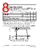
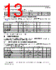
9 / 70 page  MPC8306S PowerQUICC II Pro Integrated Communications Processor Family Hardware Specifications, Rev. 1 Freescale Semiconductor 9 Electrical Characteristics 2.1.3 Output Driver Characteristics The following table provides information on the characteristics of the output driver strengths. 2.1.4 Input Capacitance Specification The following table describes the input capacitance for the SYS_CLK_IN pin in the MPC8306S. 2.2 Power Sequencing The device does not require the core supply voltage (VDD) and I/O supply voltages (GVDD and OVDD) to be applied in any particular order. Note that during power ramp-up, before the power supplies are stable and if the I/O voltages are supplied before the core voltage, there might be a period of time that all input and output pins are actively driven and cause contention and excessive current. In order to avoid actively driving the I/O pins and to eliminate excessive current draw, apply the core voltage (VDD) before the I/O voltage (GVDD and OVDD) and assert PORESET before the power supplies fully ramp up. In the case where the core voltage is applied first, the core voltage supply must rise to 90% of its nominal value before the I/O supplies reach 0.7 V; see Figure 3. Once both the power supplies (I/O voltage and core voltage) are stable, wait for a minimum of 32 clock cycles before negating PORESET. NOTE There is no specific power down sequence requirement for the device. I/O voltage supplies (GVDD and OVDD) do not have any ordering requirements with respect to one another. Table 3. Output Drive Capability Driver Type Output Impedance ( ) Supply Voltage (V) Local bus interface utilities signals 42 OVDD =3.3 DDR2 signal 18 GVDD =1.8 DUART, system control, I2C, SPI, JTAG 42 OVDD =3.3 GPIO signals 42 OVDD =3.3 Table 4. Input Capacitance Specification Parameter/Condition Symbol Min Max Unit Note Input capacitance for all pins except SYS_CLK_IN and QE_CLK_IN CI 68 pF — Input capacitance for SYS_CLK_IN and QE_CLK_IN CICLK_IN 10 — pF 1 Note: 1. The external clock generator should be able to drive 10 pF. |
|
링크 URL |
| ALLDATASHEET 가 귀하에 도움이 되셨나요? [ DONATE ] |
Alldatasheet는? | 광고문의 | 운영자에게 연락하기 | 개인정보취급방침 | 링크 투 데이터시트 | 링크교환 | 제조사별 검색 All Rights Reserved©Alldatasheet.com |
| Russian : Alldatasheetru.com | Korean : Alldatasheet.co.kr | Spanish : Alldatasheet.es | French : Alldatasheet.fr | Italian : Alldatasheetit.com Portuguese : Alldatasheetpt.com | Polish : Alldatasheet.pl | Vietnamese : Alldatasheet.vn Indian : Alldatasheet.in | Mexican : Alldatasheet.com.mx | British : Alldatasheet.co.uk | New Zealand : Alldatasheet.co.nz |
|
Family Site : ic2ic.com |
icmetro.com |
 Korean ▼
 English
 Chinese
 German
 Japanese
 Russian
 Korean
 Spanish
 French
 Italian
 Portuguese
 Polish
 Vietnamese
 Indian
 Mexican
 British
 New Zealand