|
전자부품 데이터시트 검색엔진 |
|
|
전자부품 데이터시트 검색엔진 |
|
TMP86CS49FG 데이터시트(PDF) 195 Page - Toshiba Semiconductor |
|
|
|||||||||||||||||||||||||||||
TMP86CS49FG 데이터시트(HTML) 195 Page - Toshiba Semiconductor |
|
|
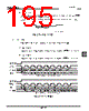
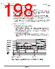
195 / 252 page  Page 181 TMP86CS49FG (2) External clock When an external clock is selected by setting SIO2CR<SCK> to “111B”, the clock via the SCK2 pin from an external source is used as the serial clock. To ensure shift operation, the serial clock pulse width must be 4/fc or more for both “H” and “L” levels. Figure 15-3 External Clock 15.3.1.2 Shift edge The leading edge is used to transmit data, and the trailing edge is used to receive data. (1) Leading edge shift Data is shifted on the leading edge of the serial clock (falling edge of the SCK2 pin input/output). (2) Trailing edge shift Data is shifted on the trailing edge of the serial clock (rising edge of the SCK2 pin input/output). Figure 15-4 Shift Edge tSCKL tSCKH tSCKL, tSCKH > 4/fc SCK2 pin 7******* ******** Bit7 Shift out ***01234 **012345 *0123456 Bit5 Bit6 Bit5 Bit6 Bit7 67****** 567***** (a) Leading edge shift (Example of MSB transfer) (b) Trailing edge shift (Example of MSB transfer) 01234567 ****0123 *****012 ******01 *******0 ******** Bit4 4567**** 34567*** 234567** 1234567* 01234567 Bit4 Bit3 Bit2 Bit1 Bit0 Bit3 Bit2 Bit1 Bit0 SIO2CR<SIOS> SCK2 pin Shift register SO2 pin Shift register SCK2 pin SI2 pin SIO2CR<SIOS> |
|
링크 URL |
| ALLDATASHEET 가 귀하에 도움이 되셨나요? [ DONATE ] |
Alldatasheet는? | 광고문의 | 운영자에게 연락하기 | 개인정보취급방침 | 링크 투 데이터시트 | 링크교환 | 제조사별 검색 All Rights Reserved©Alldatasheet.com |
| Russian : Alldatasheetru.com | Korean : Alldatasheet.co.kr | Spanish : Alldatasheet.es | French : Alldatasheet.fr | Italian : Alldatasheetit.com Portuguese : Alldatasheetpt.com | Polish : Alldatasheet.pl | Vietnamese : Alldatasheet.vn Indian : Alldatasheet.in | Mexican : Alldatasheet.com.mx | British : Alldatasheet.co.uk | New Zealand : Alldatasheet.co.nz |
|
Family Site : ic2ic.com |
icmetro.com |
 Korean ▼
 English
 Chinese
 German
 Japanese
 Russian
 Korean
 Spanish
 French
 Italian
 Portuguese
 Polish
 Vietnamese
 Indian
 Mexican
 British
 New Zealand