|
전자부품 데이터시트 검색엔진 |
|
|
전자부품 데이터시트 검색엔진 |
|
ISL9301 데이터시트(PDF) 9 Page - Intersil Corporation |
|
|
|||||||||||||||||||||||||||||
ISL9301 데이터시트(HTML) 9 Page - Intersil Corporation |
|
|
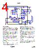
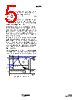
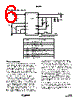
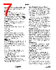
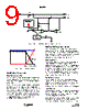
9 / 12 page  9 FN6435.0 February 25, 2008 Applications Information Input Bypass Capacitor The input capacitor is required to suppress the power supply transient response during transitions. Typically, a 10µF or larger capacitor should be sufficient to suppress the power supply noise. Due to the inductance of the power leads of the wall adapter or USB source, the input capacitor type must be properly selected to prevent high voltage transient during a hot-plug event. A tantalum capacitor is a good choice for its high ESR, providing damping to the voltage transient. Multi-layer ceramic capacitors, however, have a very low ESR and hence when chosen as input capacitor, a 1 Ω series resistor must be used (as shown in the “Typical Application Circuit” on page 6) to provide adequate damping. VOUT and VBAT Capacitor Selection The criteria for selecting the capacitor at the VOUT and VBAT pins is to maintain the stability as well as to bypass any transient load current. The recommended capacitance is a 4.7µF X5R ceramic capacitor for VOUT and 1µF for VBAT. The actual capacitance connected to the output is dependent on the actual application requirement. Layout Guidance The ISL9301 uses a thermally-enhanced DFN package that has an exposed thermal pad at the bottom side of the package. The layout should connect as much as possible to copper on the exposed pad. Typically, the component layer is more effective in dissipating heat. The thermal impedance can be further reduced by using other layers of copper connecting to the exposed pad through a thermal via array. Each thermal via is recommended to have 0.3mm diameter and 1mm distance from other thermal vias. Input Power Sources The input power source is typically a well-regulated wall cube with 1m length wire or a USB port. The input voltage ranges from 4.3V to 10V. The ISL9301 can withstand up to 28V on the input without damaging the IC. If the input voltage is higher than the OVP threshold, the IC is disabled. State Diagram The state diagram is shown in Figure 6. There are 8 states to cover all the operation modes, including the Trickle Charge, Batt Discharge, PPM, CV Charge, Charge Fault, Charge Complete, Disabled and OTP states. The IC starts with a trickle charge or constant current charge state depending on VBAT when input power is applied. In the Trickle Charge state, the PPR is LO and the CHG is LO, VOUT X3 X3 VIN IR TEMPERATURE MONITORING IT X3 VBAT + - VREF VA + - CA ISEN IREF CONTROL IREF REF Q1 Q2 FIGURE 4. CHARGE CURRENT THERMAL FOLDBACK CIRCUIT TEMPERATURE 115°C IT IR ISEN -40mA/°C FIGURE 5. CHARGE CURRENT FOLDBACK ISL9301 |
|
|
링크 URL |
| ALLDATASHEET 가 귀하에 도움이 되셨나요? [ DONATE ] |
Alldatasheet는? | 광고문의 | 운영자에게 연락하기 | 개인정보취급방침 | 링크 투 데이터시트 | 링크교환 | 제조사별 검색 All Rights Reserved©Alldatasheet.com |
| Russian : Alldatasheetru.com | Korean : Alldatasheet.co.kr | Spanish : Alldatasheet.es | French : Alldatasheet.fr | Italian : Alldatasheetit.com Portuguese : Alldatasheetpt.com | Polish : Alldatasheet.pl | Vietnamese : Alldatasheet.vn Indian : Alldatasheet.in | Mexican : Alldatasheet.com.mx | British : Alldatasheet.co.uk | New Zealand : Alldatasheet.co.nz |
|
Family Site : ic2ic.com |
icmetro.com |
 Korean ▼
 English
 Chinese
 German
 Japanese
 Russian
 Korean
 Spanish
 French
 Italian
 Portuguese
 Polish
 Vietnamese
 Indian
 Mexican
 British
 New Zealand