|
전자부품 데이터시트 검색엔진 |
|
|
전자부품 데이터시트 검색엔진 |
|
EM62100AGH 데이터시트(PDF) 19 Page - ELAN Microelectronics Corp |
|
|
|||||||||||||||||||||||||||||
EM62100AGH 데이터시트(HTML) 19 Page - ELAN Microelectronics Corp |
|
|
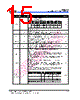
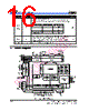
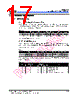
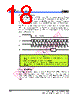
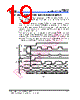
19 / 60 page  EM62100 65 COM/132 SEG STN LCD Driver Product Specification (V1.1) 09.13.2005 •••• 13 (This specification is subject to change without further notice) 6.2 Access to Display Data RAM and Internal Registers To match operation frequencies between the MPU and display RAM or internal register, the EM62100 performs an LSI-LSI pipelining via the bus holder attached to the internal data bus. When the MPU writes data to the display RAM, once the data is stored in the bus holder, then it is written to the display RAM before the next data write cycle. Moreover, when the MPU reads the display RAM, the first data read cycle (dummy) stores the read data in the bus holder, and then the data is read from the bus holder to the system bus at the next data read cycle. There is a certain restriction in the read sequence of the display RAM. It should be noted that data of the specified address is not generated by the read instruction issued immediately after the address setup. This data is generated during the second time data read. Thus, a dummy read is required whenever the address setup or the write cycle operation is performed. This relationship is shown in Figure 3. N N N N N N+1 N+2 N N N+1 N+2 Set Address n Dummy Read Data read address n Data read address n+1 RS E RW DATA MPU Address Preset Internal Timing Read Signal BUS Holder Column Address Preset Incremented Fig. 3 |
|
링크 URL |
| ALLDATASHEET 가 귀하에 도움이 되셨나요? [ DONATE ] |
Alldatasheet는? | 광고문의 | 운영자에게 연락하기 | 개인정보취급방침 | 링크 투 데이터시트 | 링크교환 | 제조사별 검색 All Rights Reserved©Alldatasheet.com |
| Russian : Alldatasheetru.com | Korean : Alldatasheet.co.kr | Spanish : Alldatasheet.es | French : Alldatasheet.fr | Italian : Alldatasheetit.com Portuguese : Alldatasheetpt.com | Polish : Alldatasheet.pl | Vietnamese : Alldatasheet.vn Indian : Alldatasheet.in | Mexican : Alldatasheet.com.mx | British : Alldatasheet.co.uk | New Zealand : Alldatasheet.co.nz |
|
Family Site : ic2ic.com |
icmetro.com |
 Korean ▼
 English
 Chinese
 German
 Japanese
 Russian
 Korean
 Spanish
 French
 Italian
 Portuguese
 Polish
 Vietnamese
 Indian
 Mexican
 British
 New Zealand