|
전자부품 데이터시트 검색엔진 |
|
|
전자부품 데이터시트 검색엔진 |
|
EM62100AGH 데이터시트(PDF) 20 Page - ELAN Microelectronics Corp |
|
|
|||||||||||||||||||||||||||||
EM62100AGH 데이터시트(HTML) 20 Page - ELAN Microelectronics Corp |
|
|
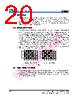
20 / 60 page  EM62100 65 COM/132 SEG STN LCD Driver 14 • ••• Product Specification (V1.1) 09.13.2005 (This specification is subject to change without further notice) 6.3 Busy Flag The busy flag is output to pin D7 by a read status command. When the busy flag is “1” it indicates that the EM62100 chip is executing its internal operations, any command other than status read is ignored during this time. If the cycle time (tCYC) is correct, this flag need not be checked before each instruction. This makes vast improvements in MPU processing capabilities possible. 6.4 Display Data RAM The display data RAM stores the pixel data for the LCD. It is a 65 ×132 addressable array. It allows access to the desired bit by specifying the page address and the column address. The 65 rows are divided into 8 pages of 8 lines and the 9th page with a single line (D0). The D7 to D0 display data from the MPU corresponds to the LCD common lines as show in Fig.4. There are few constraints at the time of display data transfer when multiple EM62100 chip is used. However, the display structures can be created easily and with a high degree of freedom. Reading from and writing to the display RAM from the MPU side is performed through the I/O buffer, which is an independent operation from signal reading for the liquid crystal driver. Consequently, even if the display data RAM is accessed asynchronously, it will not cause adverse effects on the display (such as flickering). 0 0 0 0 1 1 1 1 1 1 1 1 1 0 0 0 0 0 0 0 0 0 0 0 0 D0 D1 D2 D3 D4 COM0 COM1 COM2 COM3 COM4 Display Data RAM Liquid Crystal Display Fig. 4 6.5 Page Address Circuit The page address of the display data RAM is specified through the Page Address Set Command. The page address needs to be specified again in accessing other pages. Page address 8 is the page for the RAM region used only by the static indicators, and only display data D0 is used. |
|
링크 URL |
| ALLDATASHEET 가 귀하에 도움이 되셨나요? [ DONATE ] |
Alldatasheet는? | 광고문의 | 운영자에게 연락하기 | 개인정보취급방침 | 링크 투 데이터시트 | 링크교환 | 제조사별 검색 All Rights Reserved©Alldatasheet.com |
| Russian : Alldatasheetru.com | Korean : Alldatasheet.co.kr | Spanish : Alldatasheet.es | French : Alldatasheet.fr | Italian : Alldatasheetit.com Portuguese : Alldatasheetpt.com | Polish : Alldatasheet.pl | Vietnamese : Alldatasheet.vn Indian : Alldatasheet.in | Mexican : Alldatasheet.com.mx | British : Alldatasheet.co.uk | New Zealand : Alldatasheet.co.nz |
|
Family Site : ic2ic.com |
icmetro.com |
 Korean ▼
 English
 Chinese
 German
 Japanese
 Russian
 Korean
 Spanish
 French
 Italian
 Portuguese
 Polish
 Vietnamese
 Indian
 Mexican
 British
 New Zealand