|
전자부품 데이터시트 검색엔진 |
|
|
전자부품 데이터시트 검색엔진 |
|
AD8335 데이터시트(PDF) 17 Page - Analog Devices |
|
|
|||||||||||||||||||||||||||||
AD8335 데이터시트(HTML) 17 Page - Analog Devices |
|
|
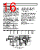
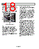
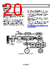
17 / 24 page  AD8335 Rev. 0 | Page 17 of 24 PREAMP Although the preamp signal path is fully differential, the design is optimized for single-ended input drive and signal source resistance matching. Thus, the negative input to the differential preamplifier Pins PMDx must be ac-grounded to provide a balanced differential signal at the PrA outputs. Detailed information regarding the preamplifier architecture is found in the LNA section of the AD8331/AD8332 data sheet. The preamplifier consists of a fixed gain amplifier with differen- tial outputs. With the negative output available and a fixed gain of 8 (18.06 dB), an active input termination is synthesized by connecting a feedback resistor between the negative output and the positive input, Pin PIPx. This technique is well known and results in the input resistance shown in Equation 2. ) 2 1 ( A R R FB IN + = (2) where A/2 is the single-ended gain, or the gain from the PIPx inputs to the PONx outputs. Since the amplifier has a gain of ×8 from its input to its differential output, it is important to note that the gain A/2 is the gain from Pin PIPx to Pin PONx, which is 6 dB lower, or 12.04 dB (×4). The input resistance is reduced by an internal bias resistor of 14.7 kΩ in parallel with the source resistance connected to Pin PIPx, with Pin PMDx ac-grounded. Equation 3 can be used to calculate the needed RFB for a desired RIN, and is used for higher values of RIN. kΩ 7 . 14 || ) 4 1 ( + = FB IN R R (3) For example, to set RIN = 200 Ω, the value of RFB is 1.013 kΩ. If the simplified Equation 2 is used to calculate RIN, the value is 197 Ω, resulting in a less than 0.1 dB gain error. Factors such as a widely varying source resistance might influence the absolute gain accuracy more significantly. At higher frequencies, the input capacitance of the PrA needs to be considered. The user must determine the level of matching accuracy and adjust RFB accordingly. The bandwidths (BW) of the preamplifier and VGA are approximately 110 MHz each, resulting in a cascaded BW of approximately 80 MHz. Ultimately the BW of the PrA limits the accuracy of the synthesized RIN. For RIN = RS up to approximately 200 Ω, the best match is between 100 kHz and 10 MHz, where the lower frequency limit is determined by the size of the ac- coupling capacitors, and the upper limit is determined by the preamplifier BW. Furthermore, the input capacitance and RS limits the BW at higher frequencies. FREQUENCY (Hz) 10 100 1k 100k 1M 10M 50M RIN = 500Ω, RFB = 2.5kΩ RSH = ∞, CSH = 0pF RIN = 200Ω, RFB = 1kΩ RSH = 50Ω, CSH = 22pF RIN = 100Ω, RFB = 499Ω RIN = 50Ω, RFB = 249Ω RSH = ∞, CSH = 0pF RSH = 50Ω, CSH = 22pF Figure 55. RIN vs. Frequency for Various Values of RFB. Effects of RSH and CSH are also shown. Figure 55 shows RIN vs. frequency for various values of RFB. Note that at the lowest value, 50 Ω, RIN peaks at frequencies greater than 10 MHz. This is due to the BW roll-off of the PrA as mentioned earlier. The RSH and CSH network shown in Figure 58 reduces this peaking. However, as can be seen for larger RIN values, parasitic capacitance starts rolling off the signal BW before the PrA can produce peaking and the RSH/CSH network further degrades the match. Therefore RSH and CSH should not be used for values of RIN greater than 50 Ω. Noise The total input referred noise (IRN) is approximately 1.3 nV/√Hz. Allowing for a gain of ×8 in the preamp, the VGA noise is 0.46 nV/√Hz referred to the PrA input. The preamp noise is 1.2 nV/√Hz. It is important to note that these noise values include all amplifier noise sources, including the VGA and the preamplifier gain resistors. Frequently, manufacturer noise specifications exclude gain setting resistors, and the voltage noise spectral density of an op amp might be presented as 1 nV/√Hz. Including the gain resistors results in a much higher noise specification. |
|
|
링크 URL |
| ALLDATASHEET 가 귀하에 도움이 되셨나요? [ DONATE ] |
Alldatasheet는? | 광고문의 | 운영자에게 연락하기 | 개인정보취급방침 | 링크 투 데이터시트 | 링크교환 | 제조사별 검색 All Rights Reserved©Alldatasheet.com |
| Russian : Alldatasheetru.com | Korean : Alldatasheet.co.kr | Spanish : Alldatasheet.es | French : Alldatasheet.fr | Italian : Alldatasheetit.com Portuguese : Alldatasheetpt.com | Polish : Alldatasheet.pl | Vietnamese : Alldatasheet.vn Indian : Alldatasheet.in | Mexican : Alldatasheet.com.mx | British : Alldatasheet.co.uk | New Zealand : Alldatasheet.co.nz |
|
Family Site : ic2ic.com |
icmetro.com |
 Korean ▼
 English
 Chinese
 German
 Japanese
 Russian
 Korean
 Spanish
 French
 Italian
 Portuguese
 Polish
 Vietnamese
 Indian
 Mexican
 British
 New Zealand