|
전자부품 데이터시트 검색엔진 |
|
|
전자부품 데이터시트 검색엔진 |
|
AD8335 데이터시트(PDF) 18 Page - Analog Devices |
|
|
|||||||||||||||||||||||||||||
AD8335 데이터시트(HTML) 18 Page - Analog Devices |
|
|
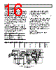
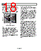
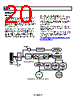
18 / 24 page  AD8335 Rev. 0 | Page 18 of 24 Figure 56 shows the simulated noise figure (NF) vs. source resistance, and various values of preamplifier RIN from 50 Ω, to 14.7 kΩ, the value seen looking into Pins PIPx when RFB = ∞. As shown in the figure, the minimum NF for RIN = 50 Ω is slightly less than 7 dB. Note that, for this preamplifier, the NF is optimized for the RIN from 50 Ω to 200 Ω; for RFB = ∞, the minimum NF is at approximately 480 Ω. This optimum noise resistance can also be calculated by dividing the input referred voltage noise by the current noise. 0 2 4 6 8 10 12 14 16 RS (Ω) 10 100 1k RIN = 50Ω RFB = 250Ω RIN = 75Ω RFB = 375Ω RIN = 100Ω RFB = 500Ω RIN = 200Ω RFB = 1kΩ RIN = 14.7kΩ RFB = ∞ SIMULATION INCLUDES NOISE OF VGA f = 1MHz Figure 56. Simulated Noise Figure vs. RS for Various Fixed Values of RIN, Actively Matched VGA As seen in Figure 54, the basic architecture, an X-AMPTM, consists of a ladder attenuator, followed by a fixed-gain amplifier with selectable input stages. Earlier examples of this architecture are to be found in the AD60x series, AD8331/ AD8332, and AD8367 VGAs. Through a proprietary, tempera- ture-compensated interpolator design, the bias currents to the input gm stages are continuously steered from right to left (decreasing attenuation) resulting in increasing gain. The HILO (HL12 and HL34) gain pins select one of two output amplifier networks consisting of the feedback resistors, amplifier stages, and buffers. Optimizing the System Dynamic Range The VGA output gain switch of 8 dB (×2.5) optimizes the VGA noise floor for a 10-bit or 12-bit ADC, assuming a full-scale ADC input voltage of 1 V p-p. At low gain the ADC SNR should limit the system noise per- formance, while at high gains the noise is defined by the source and preamplifier. The maximum voltage swing is bounded by the full-scale peak-to-peak ADC input voltage (typically 1 V p-p to 2 V p-p). The noise performance is optimized by adjusting the noise floor of the VGA according to the ADC resolution. The SNR of a 12-bit converter is theoretically 12 dB better than a 10-bit; however, approximately 8 dB is typical in practice, accounting for the 8 dB gain option of the AD8335. The IRN and the power consumption of the VGA are unaffected by either gain setting; therefore, only the output referred noise (ORN) changes (by 8 dB) without affecting any other parameters. Attenuator The attenuator is an 8-stage differential R-2R ladder with a total attenuation of 48.16 dB – 6.02 dB per tap. The effective input resistance per side is 320 Ω nominally for a total differential resistance of 640 Ω. The common-mode voltage of the attenuator and the VGA is controlled by an amplifier that uses the same midsupply voltage derived in the preamplifier, permitting dc coupling of the PrA to the VGA without introducing large offsets due to common-mode differences. However, when dc coupling between the PrA and VGA, any offset from the PrA are amplified as the gain is increased, producing an exponentially increasing VGA output offset. When the PrA and the VGA are ac-coupled, the output offset is unchanged with changes in gain (see Figure 15). As a result, ac coupling is recommended for most applications. As can be seen from Figure 54, Pins VCMx connect to the respective midpoints on each channel and are used to ac decouple the common-mode node at high frequencies. It is very important that at least a 0.1 µF capacitor be used, with better decoupling at higher frequencies when another smaller capacitor (10 nF) is connected in parallel. The internal +1 buffer provides correct common-mode bias levels and any dynamic currents have to be absorbed by the external decoupling capacitors. |
|
|
링크 URL |
| ALLDATASHEET 가 귀하에 도움이 되셨나요? [ DONATE ] |
Alldatasheet는? | 광고문의 | 운영자에게 연락하기 | 개인정보취급방침 | 링크 투 데이터시트 | 링크교환 | 제조사별 검색 All Rights Reserved©Alldatasheet.com |
| Russian : Alldatasheetru.com | Korean : Alldatasheet.co.kr | Spanish : Alldatasheet.es | French : Alldatasheet.fr | Italian : Alldatasheetit.com Portuguese : Alldatasheetpt.com | Polish : Alldatasheet.pl | Vietnamese : Alldatasheet.vn Indian : Alldatasheet.in | Mexican : Alldatasheet.com.mx | British : Alldatasheet.co.uk | New Zealand : Alldatasheet.co.nz |
|
Family Site : ic2ic.com |
icmetro.com |
 Korean ▼
 English
 Chinese
 German
 Japanese
 Russian
 Korean
 Spanish
 French
 Italian
 Portuguese
 Polish
 Vietnamese
 Indian
 Mexican
 British
 New Zealand