|
전자부품 데이터시트 검색엔진 |
|
|
전자부품 데이터시트 검색엔진 |
|
AD8335 데이터시트(PDF) 22 Page - Analog Devices |
|
|
|||||||||||||||||||||||||||||
AD8335 데이터시트(HTML) 22 Page - Analog Devices |
|
|
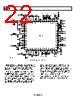
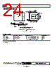
22 / 24 page  AD8335 Rev. 0 | Page 22 of 24 PIP2 CSH2 22pF RFB2 249 Ω PIP3 CSH3 22pF RFB3 249 Ω RSH3 49.9 Ω RSH4 49.9 Ω CSH4 22pF RFB4 249 Ω 120nH FB +5V VOH3 VOH4 RSH1 49.9 Ω CSH1 22pF RFB1 249 Ω VGN2 1nF* SL12 120nH FB +5V 1nF* 1nF* SL34 VGN1 H +5V L PIP4 +5V PIP1 VPP VPP +5V VOH1 VOL1 VOL2 VOH2 VOL3 VPV VPV VOL4 VGN3 VGN4 VPP VPP 1nF* 0.1 µF 0.1 µF 0.1 µF 0.1 µF 0.1 µF 0.1 µF 0.1 µF 0.1 µF 0.1 µF 0.1 µF 0.1 µF 0.1 µF 0.1 µF 0.1 µF 0.1 µF 0.1 µF 0.1 µF 0.1 µF 0.1 µF 0.1 µF 0.1 µF 0.1 µF 0.1 µF 0.1 µF 0.1 µF 0.1 µF 0.1 µF 0.1 µF 0.1 µF 0.1 µF 0.1 µF 0.1 µF 0.1 µF 0.1 µF 0.1 µF 0.1 µF 50 49 56 55 51 54 53 52 58 57 59 62 61 60 63 64 GND4 VPV2 VOL2 VOH1 VOL1 VOH2 VPV4 VOH3 VOL3 VOH4 VPV3 VOL4 VPV1 GND1 35 36 37 38 42 39 40 41 34 33 48 47 43 46 45 44 GND3 GND2 H +5V L 28 25 26 27 17 18 19 21 22 23 24 29 30 31 32 20 PMD2 PON2 PIP2 COM2 VIP2 VIN2 POP2 COM3 VIP3 VIN3 PIP3 PON3 PMD3 POP3 VPP3 VPP2 15 16 8 7 6 5 1 4 3 2 14 13 9 12 11 10 AD8335 VPP *SEE TEXT RSH2 49.9 Ω Figure 58. Basic Connections for RIN = 50 Ω The preamp PMD pins must be capacitively coupled to ground. Although the preamplifier is a differential design, the PMD pins are the internal input bias nodes and are made available for bypassing only. These pins may not be used as signal inputs. The PIPx inputs must be capacitively coupled from the signal source because they have a nominal dc level of more than half the supply voltage. AC coupling capacitors throughout the circuit should be as large as possible for the application. Although 0.1 µF capacitors are shown in Figure 58 (and used in most positions in the evaluation board), values of these capacitors should be determined by the application. Capacitors used for coupling PMDx and PIPx pins should be the same value. When synthesizing low values of RIN, the bandwidth of the preamplifier produces some peaking at the high end of the frequency response. The optional series RSHx/CSHx network shown in Figure 58 flattens the response (see Figure 55). With a 50 Ω source, the resistor and capacitor values should be 49.9 Ω and 22 pF. For RS values greater than 100 Ω, the network is not needed. The circuit is stable in either scenario. The starred capacitors in Figure 58 (*) on the VGNx pins may be removed when faster gain control signals are required. |
|
|
링크 URL |
| ALLDATASHEET 가 귀하에 도움이 되셨나요? [ DONATE ] |
Alldatasheet는? | 광고문의 | 운영자에게 연락하기 | 개인정보취급방침 | 링크 투 데이터시트 | 링크교환 | 제조사별 검색 All Rights Reserved©Alldatasheet.com |
| Russian : Alldatasheetru.com | Korean : Alldatasheet.co.kr | Spanish : Alldatasheet.es | French : Alldatasheet.fr | Italian : Alldatasheetit.com Portuguese : Alldatasheetpt.com | Polish : Alldatasheet.pl | Vietnamese : Alldatasheet.vn Indian : Alldatasheet.in | Mexican : Alldatasheet.com.mx | British : Alldatasheet.co.uk | New Zealand : Alldatasheet.co.nz |
|
Family Site : ic2ic.com |
icmetro.com |
 Korean ▼
 English
 Chinese
 German
 Japanese
 Russian
 Korean
 Spanish
 French
 Italian
 Portuguese
 Polish
 Vietnamese
 Indian
 Mexican
 British
 New Zealand