|
전자부품 데이터시트 검색엔진 |
|
|
전자부품 데이터시트 검색엔진 |
|
AD8335 데이터시트(PDF) 19 Page - Analog Devices |
|
|
|||||||||||||||||||||||||||||
AD8335 데이터시트(HTML) 19 Page - Analog Devices |
|
|
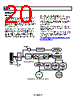
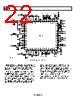
19 / 24 page  AD8335 Rev. 0 | Page 19 of 24 Gain Control The gain control interface has two inputs, VGAIN (Pins VGNx) and VSLP (Pins SLxx). The slope input is intended only as a decoupling pin, and the only guaranteed gain slope is the 20 dB/V default. However, if a voltage is applied to the VSLP inputs, the gain slope can be increased by reducing the slope voltage. For example, if a voltage of 1.67 V is applied to Pins SLxx, the gain slope changes to 30 dB/V. Use Equation 4 to calculate the gain slope. Slope VSLP dB/V 20 V 5 . 2 × = (4) VGAIN varies the gain of the VGA through the interpolator by selecting the appropriate input stages connected to the input attenuator. The nominal VGAIN range for 20 dB/V is 0 V to 3 V, with the best gain-linearity from approximately 0.5 V to 2.5 V, where the error is typically less than ±0.2 dB. For VGAIN voltages above 2.5 V and less than 0.5 V, the error increases (see Figure 4). The value of the VGAIN voltage can be increased to that of the supply voltage, without gain foldover. Each channel has separate gain control pins that can be connected to a common voltage-source such as found in most ultrasound applications. For control of individual channels, connect the appropriate gain control signal to each channel. Output Stage Duplicate output stages of the VGA provide an 8 dB (×2.5) gain switch. The gain switch is intended to optimize the output noise floor for either a 10-bit or 12-bit ADC. The VGA gain is 20 dB (×10) in LO gain mode and 28 dB (×25) in HI gain mode. The logic setting of the HILO (Pins HLxx) selects between output amplifiers including the gain resistors and feedback buffers. 100 MHz bandwidth is maintained between the amplifiers by changing the compensation capacitance as the gain switches gain settings. Power consumption is the same for either level of gain. In certain applications, power consumption can be reduced by lowering the supply voltage as much as possible; however, the output dynamic range is affected by the more limited swing. The fully differential signal path of the AD8335 restores 6 dB of dynamic range, and the common-mode level is maintained automatically at half the supply voltage for maximum signal swing. The differential signal has the added benefit of suppress- ing the even order harmonics. The output amplifier is designed to drive a nominal differential load of 500 Ω or greater; the signal swing can be as large as 5 V p-p differential before clipping occurs. However, that distor- tion increases before reaching the clipping level. Distortion is shown in Figure 25 through Figure 34 for typical values of 1 V p-p or 2 V p-p (full-scale inputs for many ADCs). The output is ac-coupled to a differential anti-alias filter driving a differential ADC. Most modern ADCs have differential inputs and achieve optimum performance when driven differentially. For more information, see the Applications section. VGA Noise As with all X-AMPs, the output noise of the VGA is constant with gain. This causes the input referred noise to increase as the gain is decreased. This characteristic is desirable in receiver applications where wide dynamic range input signals are com- pressed with a fixed ceiling and noise floor into an ADC. The VGA output noise is approximately 33 nV/√Hz in LO gain mode and 2.5 times higher than this, 83 nV/√Hz, in HI gain mode. As the gain increases, the noise of the preamplifier prevails and, at the maximum VGA gain, the output noise is approxi- mately 90 nV/√Hz and 225 nV/√Hz for LO and HI gain modes, respectively. The output SNR is determined by the noise floor and the largest signal level, typically limited by the FS of the ADC. Modulation noise, essentially the noise introduced by the gain control input, can be troublesome. Normally one tends to look at the main amplifier signal path for noise, but a VGA is really a multiplier with the following function REF IN GAIN OUT V V V V × = (4) where VREF (bias) and VGAIN (gain control interface) are both noise contributors under certain conditions. It is therefore important that the gain control signals be kept clean, especially at higher gain control slopes. |
|
|
링크 URL |
| ALLDATASHEET 가 귀하에 도움이 되셨나요? [ DONATE ] |
Alldatasheet는? | 광고문의 | 운영자에게 연락하기 | 개인정보취급방침 | 링크 투 데이터시트 | 링크교환 | 제조사별 검색 All Rights Reserved©Alldatasheet.com |
| Russian : Alldatasheetru.com | Korean : Alldatasheet.co.kr | Spanish : Alldatasheet.es | French : Alldatasheet.fr | Italian : Alldatasheetit.com Portuguese : Alldatasheetpt.com | Polish : Alldatasheet.pl | Vietnamese : Alldatasheet.vn Indian : Alldatasheet.in | Mexican : Alldatasheet.com.mx | British : Alldatasheet.co.uk | New Zealand : Alldatasheet.co.nz |
|
Family Site : ic2ic.com |
icmetro.com |
 Korean ▼
 English
 Chinese
 German
 Japanese
 Russian
 Korean
 Spanish
 French
 Italian
 Portuguese
 Polish
 Vietnamese
 Indian
 Mexican
 British
 New Zealand