|
전자부품 데이터시트 검색엔진 |
|
|
전자부품 데이터시트 검색엔진 |
|
AD8335 데이터시트(PDF) 23 Page - Analog Devices |
|
|
|||||||||||||||||||||||||||||
AD8335 데이터시트(HTML) 23 Page - Analog Devices |
|
|
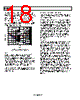
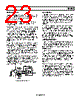
23 / 24 page  AD8335 Rev. 0 | Page 23 of 24 INPUT OVERDRIVE Excellent overload behavior is of primary importance in ultra- sound. Both the preamplifier and VGA have built-in overdrive protection and quickly recover after an overload event. Input Overload Protection As with any amplifier, voltage clamping prior to the inputs is highly recommended if the application is subject to high transient voltages. A block diagram of a simplified ultrasound transducer interface is shown in Figure 59. A common transducer element serves the dual functions of transmit and receive of ultrasound energy. During the transmit phase, high voltage pulses are applied to the ceramic elements. A typical T/R (transmit/receive) switch may consist of four high voltage diodes in a bridge configuration. Although they ideally block transmit pulses from the sensitive receiver input, diode characteristics are not ideal, and resulting leakage transients impinging on the PIPx inputs can be problematic. Since ultrasound is a pulse system, and time-of-flight is used to determine depth, quick recovery from input overloads is essential. Overload can occur in the preamp and the VGA. Immediately following a transmit pulse, the typical VGA gains are low, and the PrA is subject to overload from T/R switch leakage. With increasing gain, the VGA can become overloaded from strong echoes that occur with near field echoes and acoustically dense materials, such as bone. Figure 59 illustrates an external overload protection scheme. A pair of back-to-back Schottky diodes is installed prior to installing the ac-coupling capacitors. Although the BAS40 is shown, many types are available and merit investigation by the user. With such diodes, clamping levels of ±0.5 V or less greatly enhance the system overload performance. PrA 18dB Rs TRANSDUCER –HV BAS40-04 PMDx PIPx PONx POPx OPTIONAL SCHOTTKY OVERLOAD CLAMP RFB 3 2 1 +HV Figure 59. Input Overload Protection LOGIC INPUTS The enable Pins EN12 and EN34, the preamp shutdown Pins SP12 and SP34, and the HILO Pins HL12 and HL34 are all logic inputs of the AD8335. The enable inputs turn on and off each of the corresponding pairs of channels; the preamp shutdown pins do the same for the preamplifiers only; inputs HL12 and HL34 set the HILO gain for Channels 1 and 2, and Channels 3 and 4, respectively. Shutting down the preamplifiers allows use of the VGAs alone, while reducing power consumption. The VGAs cannot be shut down independently. The SPxx (shutdown preamp) pins are logic high; thus the pins are grounded to enable the preamplifiers. The pins can be enabled by connecting to the supply or to ground for fixed enable or disable, or to the output of a logic device. Be sure to check the data sheet of the device for voltage and current requirements. COMMON-MODE PINS The common-mode Pins VCMx are provided for bypassing the internal common-mode reference for each channel to ground. They require a capacitor at each of the four pins and can neither be connected together nor driven by an external source. DRIVING ADCs The AD8335 VGA is designed to drive 10-bit and 12-bit ADCs with minimal extra components. Because the AD8335 is a single supply 5 V part and many of the newest ADCs operate from a 3 V supply, dissimilar common-mode voltages exist between the VGA output and the ADC input. This level shift is most easily accommodated by ac coupling, especially if the signal is filtered, as is the case in most ultrasound and communications applications. When an anti-aliasing filter (AAF) is called for, it is advantageous to implement a differential configuration. A fully differential AAF requires approximately 1.5 times the number of components than a single-ended filter, because the components that in the single-ended case are tied to ground, now connect across the differential signal path. Although the series components double, the component count for the differential filter is more economical when compared to simply building a pair of single-ended filters requiring twice as many components. |
|
|
링크 URL |
| ALLDATASHEET 가 귀하에 도움이 되셨나요? [ DONATE ] |
Alldatasheet는? | 광고문의 | 운영자에게 연락하기 | 개인정보취급방침 | 링크 투 데이터시트 | 링크교환 | 제조사별 검색 All Rights Reserved©Alldatasheet.com |
| Russian : Alldatasheetru.com | Korean : Alldatasheet.co.kr | Spanish : Alldatasheet.es | French : Alldatasheet.fr | Italian : Alldatasheetit.com Portuguese : Alldatasheetpt.com | Polish : Alldatasheet.pl | Vietnamese : Alldatasheet.vn Indian : Alldatasheet.in | Mexican : Alldatasheet.com.mx | British : Alldatasheet.co.uk | New Zealand : Alldatasheet.co.nz |
|
Family Site : ic2ic.com |
icmetro.com |
 Korean ▼
 English
 Chinese
 German
 Japanese
 Russian
 Korean
 Spanish
 French
 Italian
 Portuguese
 Polish
 Vietnamese
 Indian
 Mexican
 British
 New Zealand