|
전자부품 데이터시트 검색엔진 |
|
|
전자부품 데이터시트 검색엔진 |
|
TMP86CS49FG 데이터시트(PDF) 219 Page - Toshiba Semiconductor |
|
|
|||||||||||||||||||||||||||||
TMP86CS49FG 데이터시트(HTML) 219 Page - Toshiba Semiconductor |
|
|
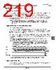
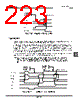
219 / 252 page  Page 205 TMP86CS49FG 16.6 Data Transfer of I2C Bus 16.6.1 Device initialization For initialization of device, set the ACK in SBICRA to “1” and the BC to “000”. Specify the data length to 8 bits to count clocks for an acknowledge signal. Set a transfer frequency to the SCK in SBICRA. Next, set the slave address to the SA in I2CAR and clear the ALS to “0” to set an addressing format. After confirming that the serial bus interface pin is high level, for specifying the default setting to a slave receiver mode, clear “0” to the MST, TRX and BB in SBICRB, set “1” to the PIN, “10” to the SBIM, and “00” to bits SWRST1 and SWRST0. Note:The initialization of a serial bus interface circuit must be complete within the time from all devices which are connected to a bus have initialized to and device does not generate a start condition. If not, the data can not be received correctly because the other device starts transferring before an end of the initialization of a serial bus interface circuit. 16.6.2 Start condition and slave address generation Confirm a bus free status (BB = 0). Set the ACK to “1” and specify a slave address and a direction bit to be transmitted to the SBIDBR. By writing “1” to the MST, TRX, BB and PIN, the start condition is generated on a bus and then, the slave address and the direction bit which are set to the SBIDBR are output. The time from generating the START condition until the falling SCL pin takes tLOW. An INTSBI interrupt request occurs at the 9th falling edge of a SCL clock cycle, and the PIN is cleared to “0”. The SCL pin is pulled-down to the low level while the PIN is “0”. When an interrupt request occurs, the TRX changes by the hardware according to the direction bit only when an acknowledge signal is returned from the slave device. Note 1: Do not write a slave address to be output to the SBIDBR while data is transferred. If data is written to the SBIDBR, data to been outputting may be destroyed. Note 2: The bus free must be confirmed by software within 98.0 µs (The shortest transmitting time according to the I2C bus standard) after setting of the slave address to be output. Only when the bus free is confirmed, set "1" to the MST, TRX, BB, and PIN to generate the start conditions. If the writing of slave address and setting of MST, TRX, BB and PIN doesn't finish within 98.0 µs, the other masters may start the transferring and the slave address data written in SBIDBR may be broken. Figure 16-9 Start Condition Generation and Slave Address Transfer 16.6.3 1-word data transfer Check the MST by the INTSBI interrupt process after an 1-word data transfer is completed, and determine whether the mode is a master or slave. Start condition Slave address + Direction bit A6 A5 2 3 4 5 6 7 8 9 A4 A3 A2 A1 A0 R/W 1 Acknowledge signal from a slave device SCL pin SDA pin PIN INTSBI interrupt request |
|
링크 URL |
| ALLDATASHEET 가 귀하에 도움이 되셨나요? [ DONATE ] |
Alldatasheet는? | 광고문의 | 운영자에게 연락하기 | 개인정보취급방침 | 링크 투 데이터시트 | 링크교환 | 제조사별 검색 All Rights Reserved©Alldatasheet.com |
| Russian : Alldatasheetru.com | Korean : Alldatasheet.co.kr | Spanish : Alldatasheet.es | French : Alldatasheet.fr | Italian : Alldatasheetit.com Portuguese : Alldatasheetpt.com | Polish : Alldatasheet.pl | Vietnamese : Alldatasheet.vn Indian : Alldatasheet.in | Mexican : Alldatasheet.com.mx | British : Alldatasheet.co.uk | New Zealand : Alldatasheet.co.nz |
|
Family Site : ic2ic.com |
icmetro.com |
 Korean ▼
 English
 Chinese
 German
 Japanese
 Russian
 Korean
 Spanish
 French
 Italian
 Portuguese
 Polish
 Vietnamese
 Indian
 Mexican
 British
 New Zealand