 |
전자부품 데이터시트 검색엔진 |
|
|
전자부품 데이터시트 검색엔진 |
|
The question interval is too short.
Please try again in a few seconds.

Hello, Please ask a question about PIC24F16KA102 Datasheet
# Example questions:
➢ Describe the role of the wr bit (bit 15 of nvmcon) in the icsp programming cycle, and how it is used to determine the status of erase or write operations.
➢ Explain why this format is used and how it contributes to the programming process.
➢ What is the primary purpose of using the tblpag register during the code memory writing process?
| Part No. | PIC24F16KA102 |
| Manufacturer | MICROCHIP |
| Size | 727 Kbytes |
| Pages | 48 pages |
| Description | Flash Programming Specifications |






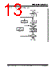




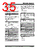







1. Introduction & General ICSP Process
️· ICSP (In-Circuit Serial Programming): A method for programming a microcontroller's memory and configuration bits via a serial interface using the PGCx (Programming Clock) and PGDx (Programming Data) pins.
️· Flow: ICSP programming involves sending a series of commands and data via the serial interface. These are often sequences of `MOV` (move), `BSET` (bit set), `NOP` (no operation) instructions.
️· LSB First: Data is transmitted Least Significant Bit first.
️· Poll the WR Bit: Programming cycles (erase/write) are self-timed. The `WR` bit in the NVMCON register must be polled (checked repeatedly) to determine when the cycle is complete.
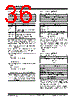
2. Erasing Program Memory (Bulk Erase)
️· Purpose: This process completely erases the microcontroller's code memory, data memory, and configuration bits.
️· Steps (Table 3-4):
- Exit Reset Vector: Immediately starts the process by leaving the reset state.
- Initialize NVMCON: Sets the NVMCON register to the correct value (4064h) to initiate the complete memory erase.
- Load TBLPAG & Dummy Table Write: This step is crucial for selecting the area of memory to erase. A dummy table write is performed as part of the process.
- Initiate Erase: Sets the WR bit in NVMCON, starting the erase cycle.
- Poll WR Bit: The program waits until the WR bit is cleared by hardware, indicating the erase is finished.
- Clock out VISI Register: The final instruction to clear the programming.
3. Writing Code Memory (Row Programming)
️· Purpose: Writes a full row (32 words) of code memory.
️· Overview: This process uses packed instruction words and a table-based writing scheme.
️· Steps (Table 3-5):
- Exit Reset Vector: As before, initializes the process.
- Initialize NVMCON: Sets NVMCON for row programming.
- Load TBLPAG & W7: Loads the starting address for programming into these registers.
- Load Packed Instruction Words: Four packed instruction words are loaded into working registers W0-W5.
- TBLWT Instructions: Eight `TBLWT` instructions are used to transfer the packed words from the working registers to the code memory write latches.
- Repeat: This sequence (steps 3-5) is repeated eight times to program an entire 32-word row of code memory.
- Initiate Programming: Sets the WR bit in NVMCON, triggering the programming cycle.
- Reset PC: The internal PC is reset to 200h to prevent unintended jumps to unimplemented memory.
- Poll WR Bit: The program waits for the WR bit to clear, indicating completion.
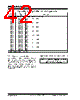
4. Configuration Registers
️· The procedure for programming Configuration registers is similar to programming Code Memory.
5. Key Registers
️· NVMCON: Controls memory erase/write operations.
️· TBLPAG: Used for selecting memory pages during programming.
️· W0-W7: Working registers used to store data temporarily during programming.
️· VISI: A register used to clear the programming.
️· PC: Program Counter, a key register that should be reset when programming to avoid issues.
Important Notes & Considerations:
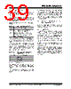
️· Packed Instruction Format: Figure 3-7 depicts the format of packed instruction words. This is important for understanding how data is organized when programming code memory.
️· Error Handling: The text doesn't cover error handling or recovery. A real-world implementation would need to include mechanisms to detect and respond to programming errors.
️· Detailed Timing: The process involves specific timing requirements on the PGCx and PGDx pins. The text doesn't elaborate on these timing details, which are critical for successful programming.
️· Device Specifics: The specific NVMCON values and other parameters might vary slightly depending on the exact PIC24FXXKAXXX microcontroller being programmed. Consult the device datasheet for precise details.
1. Introduction & General ICSP Process
️· ICSP (In-Circuit Serial Programming): A method for programming a microcontroller's memory and configuration bits via a serial interface using the PGCx (Programming Clock) and PGDx (Programming Data) pins.
️· Flow: ICSP programming involves sending a series of commands and data via the serial interface. These are often sequences of `MOV` (move), `BSET` (bit set), `NOP` (no operation) instructions.
️· LSB First: Data is transmitted Least Significant Bit first.
️· Poll the WR Bit: Programming cycles (erase/write) are self-timed. The `WR` bit in the NVMCON register must be polled (checked repeatedly) to determine when the cycle is complete.
2. Erasing Program Memory (Bulk Erase)
️· Purpose: This process completely erases the microcontroller's code memory, data memory, and configuration bits.
️· Steps (Table 3-4):
- Exit Reset Vector: Immediately starts the process by leaving the reset state.
- Initialize NVMCON: Sets the NVMCON register to the correct value (4064h) to initiate the complete memory erase.
- Load TBLPAG & Dummy Table Write: This step is crucial for selecting the area of memory to erase. A dummy table write is performed as part of the process.
- Initiate Erase: Sets the WR bit in NVMCON, starting the erase cycle.
- Poll WR Bit: The program waits until the WR bit is cleared by hardware, indicating the erase is finished.
- Clock out VISI Register: The final instruction to clear the programming.
3. Writing Code Memory (Row Programming)
️· Purpose: Writes a full row (32 words) of code memory.
️· Overview: This process uses packed instruction words and a table-based writing scheme.
️· Steps (Table 3-5):
- Exit Reset Vector: As before, initializes the process.
- Initialize NVMCON: Sets NVMCON for row programming.
- Load TBLPAG & W7: Loads the starting address for programming into these registers.
- Load Packed Instruction Words: Four packed instruction words are loaded into working registers W0-W5.
- TBLWT Instructions: Eight `TBLWT` instructions are used to transfer the packed words from the working registers to the code memory write latches.
- Repeat: This sequence (steps 3-5) is repeated eight times to program an entire 32-word row of code memory.
- Initiate Programming: Sets the WR bit in NVMCON, triggering the programming cycle.
- Reset PC: The internal PC is reset to 200h to prevent unintended jumps to unimplemented memory.
- Poll WR Bit: The program waits for the WR bit to clear, indicating completion.
4. Configuration Registers
️· The procedure for programming Configuration registers is similar to programming Code Memory.
5. Key Registers
️· NVMCON: Controls memory erase/write operations.
️· TBLPAG: Used for selecting memory pages during programming.
️· W0-W7: Working registers used to store data temporarily during programming.
️· VISI: A register used to clear the programming.
️· PC: Program Counter, a key register that should be reset when programming to avoid issues.
Important Notes & Considerations:
️· Packed Instruction Format: Figure 3-7 depicts the format of packed instruction words. This is important for understanding how data is organized when programming code memory.
️· Error Handling: The text doesn't cover error handling or recovery. A real-world implementation would need to include mechanisms to detect and respond to programming errors.
️· Detailed Timing: The process involves specific timing requirements on the PGCx and PGDx pins. The text doesn't elaborate on these timing details, which are critical for successful programming.
️· Device Specifics: The specific NVMCON values and other parameters might vary slightly depending on the exact PIC24FXXKAXXX microcontroller being programmed. Consult the device datasheet for precise details.
| Part No. | PIC24F16KA102 |
| Manufacturer | MICROCHIP |
| Size | 727 Kbytes |
| Pages | 48 pages |
| Description | Flash Programming Specifications |
| ALLDATASHEET 가 귀하에 도움이 되셨나요? [ DONATE ] |
Alldatasheet는? | 광고문의 | 운영자에게 연락하기 | 개인정보취급방침 | 링크 투 데이터시트 | 링크교환 | 제조사별 검색 All Rights Reserved©Alldatasheet.com |
| Russian : Alldatasheetru.com | Korean : Alldatasheet.co.kr | Spanish : Alldatasheet.es | French : Alldatasheet.fr | Italian : Alldatasheetit.com Portuguese : Alldatasheetpt.com | Polish : Alldatasheet.pl | Vietnamese : Alldatasheet.vn Indian : Alldatasheet.in | Mexican : Alldatasheet.com.mx | British : Alldatasheet.co.uk | New Zealand : Alldatasheet.co.nz |
|
Family Site : ic2ic.com |
icmetro.com |
 Korean ▼
  English
 Chinese
 German
 Japanese
 Russian
 Spanish
 French
 Italian
 Portuguese
 Polish
 Vietnamese
 Indian
 Mexican
 British
 New Zealand