|
전자부품 데이터시트 검색엔진 |
|
|
전자부품 데이터시트 검색엔진 |
|
PIC24F16KA102 데이터시트(PDF) 11 Page - Microchip Technology |
|
|
|||||||||||||||||||||||||||||
PIC24F16KA102 데이터시트(HTML) 11 Page - Microchip Technology |
|
|
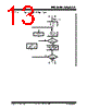
11 / 48 page  PIC24FXXKAXXX © 2008 Microchip Technology Inc. Advance Information DS39919A-page 11 FIGURE 3-7: PACKED INSTRUCTION WORDS IN W0:W5 15 8 7 0 W0 LSW0 W1 MSB1 MSB0 W2 LSW1 W3 LSW2 W4 MSB3 MSB2 W5 LSW3 TABLE 3-5: SERIAL INSTRUCTION EXECUTION FOR WRITING CODE MEMORY Command (Binary) Data (Hex) Description Step 1: Exit the Reset vector. 0000 0000 0000 000000 040200 000000 NOP GOTO 0x200 NOP Step 2: Set the NVMCON to program 32 instruction words. 0000 0000 24004A 883B0A MOV #0x4004, W10 MOV W10, NVMCON Step 3: Initialize the Write Pointer (W7) for TBLWT instruction. 0000 0000 0000 200xx0 880190 2xxxx7 MOV #<DestinationAddress23:16>, W0 MOV W0, TBLPAG MOV #<DestinationAddress15:0>, W7 Step 4: Load W0:W5 with the next 4 instruction words to program. 0000 0000 0000 0000 0000 0000 2xxxx0 2xxxx1 2xxxx2 2xxxx3 2xxxx4 2xxxx5 MOV #<LSW0>, W0 MOV #<MSB1:MSB0>, W1 MOV #<LSW1>, W2 MOV #<LSW2>, W3 MOV #<MSB3:MSB2>, W4 MOV #<LSW3>, W5 |
|
링크 URL |
| ALLDATASHEET 가 귀하에 도움이 되셨나요? [ DONATE ] |
Alldatasheet는? | 광고문의 | 운영자에게 연락하기 | 개인정보취급방침 | 링크 투 데이터시트 | 링크교환 | 제조사별 검색 All Rights Reserved©Alldatasheet.com |
| Russian : Alldatasheetru.com | Korean : Alldatasheet.co.kr | Spanish : Alldatasheet.es | French : Alldatasheet.fr | Italian : Alldatasheetit.com Portuguese : Alldatasheetpt.com | Polish : Alldatasheet.pl | Vietnamese : Alldatasheet.vn Indian : Alldatasheet.in | Mexican : Alldatasheet.com.mx | British : Alldatasheet.co.uk | New Zealand : Alldatasheet.co.nz |
|
Family Site : ic2ic.com |
icmetro.com |
 Korean ▼
 English
 Chinese
 German
 Japanese
 Russian
 Korean
 Spanish
 French
 Italian
 Portuguese
 Polish
 Vietnamese
 Indian
 Mexican
 British
 New Zealand