|
전자부품 데이터시트 검색엔진 |
|
|
전자부품 데이터시트 검색엔진 |
|
XPC8260ZUIFBC 데이터시트(PDF) 21 Page - Freescale Semiconductor, Inc |
|
|
|||||||||||||||||||||||||||||
XPC8260ZUIFBC 데이터시트(HTML) 21 Page - Freescale Semiconductor, Inc |
|
|
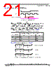
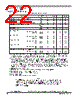
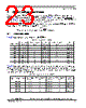
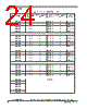
21 / 50 page  MPC8260A PowerQUICC™ II Integrated Communications Processor Hardware Specifications, Rev. 2.0 Freescale Semiconductor 21 Electrical and Thermal Characteristics Figure 11 shows signal behavior in MEMC mode. Figure 11. MEMC Mode Diagram NOTE Generally, all MPC826xA bus and system output signals are driven from the rising edge of the input clock (CLKin). Memory controller signals, however, trigger on four points within a CLKin cycle. Each cycle is divided by four internal ticks: T1, T2, T3, and T4. T1 always occurs at the rising edge, and T3 at the falling edge, of CLKin. However, the spacing of T2 and T4 depends on the PLL clock ratio selected, as shown in Table 11. Figure 12 is a graphical representation of Table 11. Figure 12. Internal Tick Spacing for Memory Controller Signals Table 11. Tick Spacing for Memory Controller Signals PLL Clock Ratio Tick Spacing (T1 Occurs at the Rising Edge of CLKin) T2 T3 T4 1:2, 1:3, 1:4, 1:5, 1:6 1/4 CLKin 1/2 CLKin 3/4 CLKin 1:2.5 3/10 CLKin 1/2 CLKin 8/10 CLKin 1:3.5 4/14 CLKin 1/2 CLKin 11/14 CLKin CLKin V_CLK Memory controller signals sp34/sp30 CLKin T1 T2 T3 T4 CLKin T1 T2 T3 T4 for 1:2.5 for 1:3.5 CLKin T1 T2 T3 T4 for 1:2, 1:3, 1:4, 1:5, 1:6 |
|
링크 URL |
| ALLDATASHEET 가 귀하에 도움이 되셨나요? [ DONATE ] |
Alldatasheet는? | 광고문의 | 운영자에게 연락하기 | 개인정보취급방침 | 링크 투 데이터시트 | 링크교환 | 제조사별 검색 All Rights Reserved©Alldatasheet.com |
| Russian : Alldatasheetru.com | Korean : Alldatasheet.co.kr | Spanish : Alldatasheet.es | French : Alldatasheet.fr | Italian : Alldatasheetit.com Portuguese : Alldatasheetpt.com | Polish : Alldatasheet.pl | Vietnamese : Alldatasheet.vn Indian : Alldatasheet.in | Mexican : Alldatasheet.com.mx | British : Alldatasheet.co.uk | New Zealand : Alldatasheet.co.nz |
|
Family Site : ic2ic.com |
icmetro.com |
 Korean ▼
 English
 Chinese
 German
 Japanese
 Russian
 Korean
 Spanish
 French
 Italian
 Portuguese
 Polish
 Vietnamese
 Indian
 Mexican
 British
 New Zealand