|
전자부품 데이터시트 검색엔진 |
|
|
전자부품 데이터시트 검색엔진 |
|
XPC8260ZUIFBC 데이터시트(PDF) 13 Page - Freescale Semiconductor, Inc |
|
|
|||||||||||||||||||||||||||||
XPC8260ZUIFBC 데이터시트(HTML) 13 Page - Freescale Semiconductor, Inc |
|
|
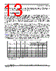
13 / 50 page  MPC8260A PowerQUICC™ II Integrated Communications Processor Hardware Specifications, Rev. 2.0 Freescale Semiconductor 13 Electrical and Thermal Characteristics where K is a constant pertaining to the particular part. K can be determined from equation (3) by measuring PD (at equilibrium) for a known TA. Using this value of K, the values of PD and TJ can be obtained by solving equations (1) and (2) iteratively for any value of TA. 2.3.1 Layout Practices Each VCC pin should be provided with a low-impedance path to the board’s power supply. Each ground pin should likewise be provided with a low-impedance path to ground. The power supply pins drive distinct groups of logic on chip. The VCC power supply should be bypassed to ground using at least four 0.1 µF by-pass capacitors located as close as possible to the four sides of the package. The capacitor leads and associated printed circuit traces connecting to chip VCC and ground should be kept to less than half an inch per capacitor lead. A four-layer board is recommended, employing two inner layers as VCC and GND planes. All output pins on the MPC826xA have fast rise and fall times. Printed circuit (PC) trace interconnection length should be minimized in order to minimize overdamped conditions and reflections caused by these fast output switching times. This recommendation particularly applies to the address and data buses. Maximum PC trace lengths of six inches are recommended. Capacitance calculations should consider all device loads as well as parasitic capacitances due to the PC traces. Attention to proper PCB layout and bypassing becomes especially critical in systems with higher capacitive loads because these loads create higher transient currents in the VCC and GND circuits. Pull up all unused inputs or signals that will be inputs during reset. Special care should be taken to minimize the noise levels on the PLL supply pins. Table 5 provides preliminary, estimated power dissipation for various configurations. Note that suitable thermal management is required for conditions above PD = 3 W (when the ambient temperature is 70 °C or greater) to ensure the junction temperature does not exceed the maximum specified value. Also note that the I/O power should be included when determining whether to use a heat sink. Table 5. Estimated Power Dissipation for Various Configurations1 1 Test temperature = room temperature (25° C) Bus (MHz) CPM Multiplier Core CPU Multiplier CPM (MHz) CPU (MHz) PINT(W) 2 2 P INT = IDD x VDD Watts Vddl 1.8 Volts Vddl 2.0 Volts Nominal Maximum Nominal Maximum 66.66 2 3 133 200 1.2 2 1.8 2.3 66.66 2.5 3 166 200 1.3 2.1 1.9 2.3 66.66 3 4 200 266 — — 2.3 2.9 66.66 3 4.5 200 300 — — 2.4 3.1 83.33 2 3 166 250 — — 2.2 2.8 83.33 2 3 166 250 — — 2.2 2.8 83.33 2.5 3.5 208 291 — — 2.4 3.1 |
|
링크 URL |
| ALLDATASHEET 가 귀하에 도움이 되셨나요? [ DONATE ] |
Alldatasheet는? | 광고문의 | 운영자에게 연락하기 | 개인정보취급방침 | 링크 투 데이터시트 | 링크교환 | 제조사별 검색 All Rights Reserved©Alldatasheet.com |
| Russian : Alldatasheetru.com | Korean : Alldatasheet.co.kr | Spanish : Alldatasheet.es | French : Alldatasheet.fr | Italian : Alldatasheetit.com Portuguese : Alldatasheetpt.com | Polish : Alldatasheet.pl | Vietnamese : Alldatasheet.vn Indian : Alldatasheet.in | Mexican : Alldatasheet.com.mx | British : Alldatasheet.co.uk | New Zealand : Alldatasheet.co.nz |
|
Family Site : ic2ic.com |
icmetro.com |
 Korean ▼
 English
 Chinese
 German
 Japanese
 Russian
 Korean
 Spanish
 French
 Italian
 Portuguese
 Polish
 Vietnamese
 Indian
 Mexican
 British
 New Zealand