|
전자부품 데이터시트 검색엔진 |
|
|
전자부품 데이터시트 검색엔진 |
|
MPC8309EC 데이터시트(PDF) 44 Page - Freescale Semiconductor, Inc |
|
|
|||||||||||||||||||||||||||||
MPC8309EC 데이터시트(HTML) 44 Page - Freescale Semiconductor, Inc |
|
|
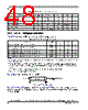
44 / 82 page  MPC8309 PowerQUICC II Pro Integrated Communications Processor Family Hardware Specifications, Rev. 0 44 Freescale Semiconductor I2C Figure 32 provides the AC test load for the I2C. Figure 32. I2C AC Test Load Figure 33 shows the AC timing diagram for the I2C bus. Figure 33. I2C Bus AC Timing Diagram Fall time of both SDA and SCL signals tI2CF 20 + 0.1 CB 4 300 ns Setup time for STOP condition tI2PVKH 0.6 — s Bus free time between a STOP and START condition tI2KHDX 1.3 — s Noise margin at the LOW level for each connected device (including hysteresis) VNL 0.1 OV DD —V Noise margin at the HIGH level for each connected device (including hysteresis) VNH 0.2 OV DD —V Notes: 1. The symbols used for timing specifications follow the pattern of t(first two letters of functional block)(signal)(state)(reference)(state) for inputs and t(first two letters of functional block)(reference)(state)(signal)(state) for outputs. For example, tI2DVKH symbolizes I 2C timing (I2) with respect to the time data input signals (D) reach the valid state (V) relative to the tI2C clock reference (K) going to the high (H) state or setup time. Also, tI2SXKL symbolizes I 2C timing (I2) for the time that the data with respect to the start condition (S) went invalid (X) relative to the tI2C clock reference (K) going to the low (L) state or hold time. Also, tI2PVKH symbolizes I 2C timing (I2) for the time that the data with respect to the stop condition (P) reaching the valid state (V) relative to the tI2C clock reference (K) going to the high (H) state or setup time. For rise and fall times, the latter convention is used with the appropriate letter: R (rise) or F (fall). 2. MPC8309 provides a hold time of at least 300 ns for the SDA signal (referred to the VIH(min) of the SCL signal) to bridge the undefined region of the falling edge of SCL. 3. The maximum tI2DVKL has only to be met if the device does not stretch the LOW period (tI2CL) of the SCL signal. 4. CB = capacitance of one bus line in pF. Table 44. I2C AC Electrical Specifications (continued) All values refer to VIH (min) and VIL (max) levels (see Table 43). Parameter Symbol1 Min Max Unit Output Z0 = 50 OVDD/2 RL = 50 Sr S SDA SCL tI2CF tI2SXKL tI2CL tI2CH tI2DXKL tI2DVKH tI2SXKL tI2SVKH tI2KHKL tI2PVKH tI2CR tI2CF PS |
|
링크 URL |
| ALLDATASHEET 가 귀하에 도움이 되셨나요? [ DONATE ] |
Alldatasheet는? | 광고문의 | 운영자에게 연락하기 | 개인정보취급방침 | 링크 투 데이터시트 | 링크교환 | 제조사별 검색 All Rights Reserved©Alldatasheet.com |
| Russian : Alldatasheetru.com | Korean : Alldatasheet.co.kr | Spanish : Alldatasheet.es | French : Alldatasheet.fr | Italian : Alldatasheetit.com Portuguese : Alldatasheetpt.com | Polish : Alldatasheet.pl | Vietnamese : Alldatasheet.vn Indian : Alldatasheet.in | Mexican : Alldatasheet.com.mx | British : Alldatasheet.co.uk | New Zealand : Alldatasheet.co.nz |
|
Family Site : ic2ic.com |
icmetro.com |
 Korean ▼
 English
 Chinese
 German
 Japanese
 Russian
 Korean
 Spanish
 French
 Italian
 Portuguese
 Polish
 Vietnamese
 Indian
 Mexican
 British
 New Zealand