|
전자부품 데이터시트 검색엔진 |
|
|
전자부품 데이터시트 검색엔진 |
|
MPC8309EC 데이터시트(PDF) 51 Page - Freescale Semiconductor, Inc |
|
|
|||||||||||||||||||||||||||||
MPC8309EC 데이터시트(HTML) 51 Page - Freescale Semiconductor, Inc |
|
|
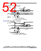
51 / 82 page  MPC8309 PowerQUICC II Pro Integrated Communications Processor Family Hardware Specifications, Rev. 0 Freescale Semiconductor 51 JTAG Figure 39 provides the AC test load for TDO and the boundary-scan outputs of the MPC8309. Figure 39. AC Test Load for the JTAG Interface Figure 40 provides the JTAG clock input timing diagram. Figure 40. JTAG Clock Input Timing Diagram Figure 41 provides the TRST timing diagram. Figure 41. TRST Timing Diagram Output hold times: Boundary-scan data TDO tJTKLDX tJTKLOX 2 2 — — ns 5 JTAG external clock to output high impedance: Boundary-scan data TDO tJTKLDZ tJTKLOZ 2 2 19 9 ns 5, 6 6 Notes: 1. All outputs are measured from the midpoint voltage of the falling/rising edge of tTCLK to the midpoint of the signal in question. The output timings are measured at the pins. All output timings assume a purely resistive 50- load (see Figure 39). Time-of-flight delays must be added for trace lengths, vias, and connectors in the system. 2. The symbols used for timing specifications follow the pattern of t(first two letters of functional block)(signal)(state)(reference)(state) for inputs and t(first two letters of functional block)(reference)(state)(signal)(state) for outputs. For example, tJTDVKH symbolizes JTAG device timing (JT) with respect to the time data input signals (D) reaching the valid state (V) relative to the tJTG clock reference (K) going to the high (H) state or setup time. Also, tJTDXKH symbolizes JTAG timing (JT) with respect to the time data input signals (D) went invalid (X) relative to the tJTG clock reference (K) going to the high (H) state. Note that, in general, the clock reference symbol representation is based on three letters representing the clock of a particular functional. For rise and fall times, the latter convention is used with the appropriate letter: R (rise) or F (fall). 3. TRST is an asynchronous level sensitive signal. The setup time is for test purposes only. 4. Non-JTAG signal input timing with respect to tTCLK. 5. Non-JTAG signal output timing with respect to tTCLK. 6. Guaranteed by design and characterization. Table 54. JTAG AC Timing Specifications (Independent of SYS_CLK_IN)1 (continued) At recommended operating conditions (see Table 2). Parameter Symbol2 Min Max Unit Notes Output Z0 = 50 OVDD/2 RL = 50 JTAG tJTKHKL tJTGR External Clock VM VM VM tJTG tJTGF VM = Midpoint Voltage (OVDD/2) TRST VM = Midpoint Voltage (OVDD/2) VM VM tTRST |
|
링크 URL |
| ALLDATASHEET 가 귀하에 도움이 되셨나요? [ DONATE ] |
Alldatasheet는? | 광고문의 | 운영자에게 연락하기 | 개인정보취급방침 | 링크 투 데이터시트 | 링크교환 | 제조사별 검색 All Rights Reserved©Alldatasheet.com |
| Russian : Alldatasheetru.com | Korean : Alldatasheet.co.kr | Spanish : Alldatasheet.es | French : Alldatasheet.fr | Italian : Alldatasheetit.com Portuguese : Alldatasheetpt.com | Polish : Alldatasheet.pl | Vietnamese : Alldatasheet.vn Indian : Alldatasheet.in | Mexican : Alldatasheet.com.mx | British : Alldatasheet.co.uk | New Zealand : Alldatasheet.co.nz |
|
Family Site : ic2ic.com |
icmetro.com |
 Korean ▼
 English
 Chinese
 German
 Japanese
 Russian
 Korean
 Spanish
 French
 Italian
 Portuguese
 Polish
 Vietnamese
 Indian
 Mexican
 British
 New Zealand