|
전자부품 데이터시트 검색엔진 |
|
|
전자부품 데이터시트 검색엔진 |
|
COP8SE 데이터시트(PDF) 30 Page - National Semiconductor (TI) |
|
|
|
|||||||||||||||||||||||||||||
COP8SE 데이터시트(HTML) 30 Page - National Semiconductor (TI) |
|
|
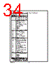
30 / 47 page  9.0 WATCHDOG/Clock Monitor (Continued) TABLE 7. WATCHDOG Service Actions Key Window Clock Action Data Data Monitor Match Match Match Valid Service: Restart Service Window Don’t Care Mismatch Don’t Care Error: Generate WATCHDOG Output Mismatch Don’t Care Don’t Care Error: Generate WATCHDOG Output Don’t Care Don’t Care Mismatch Error: Generate WATCHDOG Output 9.3 WATCHDOG AND CLOCK MONITOR SUMMARY The following salient points regarding the WATCHDOG and CLOCK MONITOR should be noted: • Both the WATCHDOG and CLOCK MONITOR detector circuits are inhibited during RESET. • Following RESET, the WATCHDOG and CLOCK MONI- TOR are both enabled, with the WATCHDOG having the maximum service window selected. • The WATCHDOG service window and CLOCK MONI- TOR enable/disable option can only be changed once, during the initial WATCHDOG service following RESET. • The initial WATCHDOG service must match the key data value in the WATCHDOG Service register WDSVR in or- der to avoid a WATCHDOG error. • Subsequent WATCHDOG services must match all three data fields in WDSVR in order to avoid WATCHDOG er- rors. • The correct key data value cannot be read from the WATCHDOG Service register WDSVR. Any attempt to read this key data value of 01100 from WDSVR will read as key data value of all 0’s. • The WATCHDOG detector circuit is inhibited during both the HALT and IDLE modes. • The CLOCK MONITOR detector circuit is active during both the HALT and IDLE modes. Consequently, the de- vice inadvertently entering the HALT mode will be de- tected as a CLOCK MONITOR error (provided that the CLOCK MONITOR enable option has been selected by the program). • With the single-pin R/C oscillator option selected and the CLKDLY bit reset, the WATCHDOG service window will resume following HALT mode from where it left off before entering the HALT mode. • With the crystal oscillator option selected, or with the single-pin R/C oscillator option selected and the CLKDLY bit set, the WATCHDOG service window will be set to its selected value from WDSVR following HALT. Conse- quently, the WATCHDOG should not be serviced for at least 2048 instruction cycles following HALT, but must be serviced within the selected window to avoid a WATCH- DOG error. • The IDLE timer T0 is not initialized with external RESET. • The user can sync in to the IDLE counter cycle with an IDLE counter (T0) interrupt or by monitoring the T0PND flag. The T0PND flag is set whenever the selected bit of the IDLE counter toggles (every 4, 8, 16, 32 or 64k in- struction cycles). The user is responsible for resetting the T0PND flag. • A hardware WATCHDOG service occurs just as the de- vice exits the IDLE mode. Consequently, the WATCH- DOG should not be serviced for at least 2048 instruction cycles following IDLE, but must be serviced within the se- lected window to avoid a WATCHDOG error. • Following RESET, the initial WATCHDOG service (where the service window and the CLOCK MONITOR enable/ disable must be selected) may be programmed any- where within the maximum service window (65,536 in- struction cycles) initialized by RESET. Note that this initial WATCHDOG service may be programmed within the ini- tial 2048 instruction cycles without causing a WATCH- DOG error. 9.4 DETECTION OF ILLEGAL CONDITIONS The device can detect various illegal conditions resulting from coding errors, transient noise, power supply voltage drops, runaway programs, etc. Reading of undefined ROM gets zeroes. The opcode for software interrupt is 00. If the program fetches instructions from undefined ROM, this will force a software interrupt, thus signaling that an illegal condition has occurred. The subroutine stack grows down for each call (jump to sub- routine), interrupt, or PUSH, and grows up for each return or POP. The stack pointer is initialized to RAM location 06F Hex during reset. Consequently, if there are more returns than calls, the stack pointer will point to addresses 070 and 071 Hex (which are undefined RAM). Undefined RAM from ad- dresses 070 to 07F (Segment 0), and all other segments (i.e., Segments 4 … etc.) is read as all 1’s, which in turn will cause the program to return to address 7FFF Hex. It is rec- ommended that the user either leave this location unpro- grammed or place an INTR instruction (all 0’s) in this location to generate a software interrupt signaling an illegal condition. Thus, the chip can detect the following illegal conditions: 1. Executing from undefined ROM. 2. Over “POP”ing the stack by having more returns than calls. When the software interrupt occurs, the user can re-initialize the stack pointer and do a recovery procedure before restart- ing (this recovery program is probably similar to that follow- ing reset, but might not contain the same program initializa- tion procedures). The recovery program should reset the software interrupt pending bit using the RPND instruction. www.national.com 30 |
|
링크 URL |
| ALLDATASHEET 가 귀하에 도움이 되셨나요? [ DONATE ] |
Alldatasheet는? | 광고문의 | 운영자에게 연락하기 | 개인정보취급방침 | 링크 투 데이터시트 | 링크교환 | 제조사별 검색 All Rights Reserved©Alldatasheet.com |
| Russian : Alldatasheetru.com | Korean : Alldatasheet.co.kr | Spanish : Alldatasheet.es | French : Alldatasheet.fr | Italian : Alldatasheetit.com Portuguese : Alldatasheetpt.com | Polish : Alldatasheet.pl | Vietnamese : Alldatasheet.vn Indian : Alldatasheet.in | Mexican : Alldatasheet.com.mx | British : Alldatasheet.co.uk | New Zealand : Alldatasheet.co.nz |
|
Family Site : ic2ic.com |
icmetro.com |
 Korean ▼
 English
 Chinese
 German
 Japanese
 Russian
 Korean
 Spanish
 French
 Italian
 Portuguese
 Polish
 Vietnamese
 Indian
 Mexican
 British
 New Zealand