|
전자부품 데이터시트 검색엔진 |
|
|
전자부품 데이터시트 검색엔진 |
|
COP8SE 데이터시트(PDF) 9 Page - National Semiconductor (TI) |
|
|
|
|||||||||||||||||||||||||||||
COP8SE 데이터시트(HTML) 9 Page - National Semiconductor (TI) |
|
|
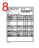
9 / 47 page  AC Electrical Characteristics −40˚C ≤ T A ≤ +135˚C unless otherwise specified. Parameter Conditions Min Typ Max Units Instruction Cycle Time (t C) Crystal/Resonator, External 4.5V ≤ V CC ≤ 5.5V 1 DC µs R/C Oscillator (Internal) 4.5V ≤ V CC ≤ 5.5V 3 DC µs Frequency Variation (Note 22), (Note 21) 4.5V ≤ V CC ≤ 5.5V ±20 % CKI Clock Duty Cycle (Note 22) fr = Max 45 55 % Rise Time (Note 22) fr = 10 MHz Ext Clock 12 ns Fall Time (Note 22) fr = 10 MHz Ext Clock 8 ns EERAM Write Cycle 715 ms Delay from Power-up to first EERAM Write Cycle 65 µs Output Propagation Delay (Note 21) R L = 2.2k, CL = 100 pF t PD1,tPD0 SO, SK 4.5V ≤ V CC ≤ 5.5V 0.7 µs All Others 4.5V ≤ V CC ≤ 5.5V 1.0 µs MICROWIRE Setup Time (t UWS) (Note 25) 20 ns MICROWIRE Hold Time (t UWH) (Note 25) 56 ns MICROWIRE Output Propagation Delay (t UPD) (Note 25) 220 ns Input Pulse Width (Note 22) Interrupt Input High Time 1 t C Interrupt Input Low Time 1 t C Timer 1 Input High Time 1 t C Timer 1 Input Low Time 1 t C Reset Pulse Width 1 µs Note 16: tC = Instruction cycle time. Note 17: Maximum rate of voltage change must be < 0.5 V/ms. Note 18: Supply and IDLE currents are measured with CKI driven with a square wave Oscillator, CKO driven 180˚ out of phase with CKI, inputs connected to VCC and outputs driven low but not connected to a load. Note 19: The HALT mode will stop CKI from oscillating in the R/C and the Crystal configurations. In the R/C configuration, CKI is forced high internally. In the crystal configuration, CKI is TRI-STATE. Measurement of IDD HALT is done with device neither sourcing nor sinking current; with L, G0, and G2–G5 programmed as low out- puts and not driving a load; all outputs programmed low and not driving a load; all inputs tied to VCC; clock monitor disabled. Parameter refers to HALT mode entered via setting bit 7 of the G Port data register. Note 20: Pins G6 and RESET are designed with a high voltage input network. These pins allow input voltages > VCC and the pins will have sink current to VCC when biased at voltages > VCC (the pins do not have source current when biased at a voltage below VCC). The effective resistance to VCC is 750Ω (typical). These two pins will not latch up. The voltage at the pins must be limited to < 14V. WARNING: Voltages in excess of 14V will cause damage to the pins. This warning excludes ESD transients. Note 21: The output propagation delay is referenced to the end of the instruction cycle where the output change occurs. Note 22: Parameter characterized but not tested. Note 23: Rise times faster than the minimum specification may trigger an internal power-on-reset. Note 24: Exclusive of R and C variation. Note 25: MICROWIRE Setup and Hold Times and Propagation Delays are referenced to the appropriate edge of the MICROWIRE clock. See Figure 4 and the MI- CROWIRE operation description. DS100973-9 FIGURE 4. MICROWIRE/PLUS Timing www.national.com 9 |
|
링크 URL |
| ALLDATASHEET 가 귀하에 도움이 되셨나요? [ DONATE ] |
Alldatasheet는? | 광고문의 | 운영자에게 연락하기 | 개인정보취급방침 | 링크 투 데이터시트 | 링크교환 | 제조사별 검색 All Rights Reserved©Alldatasheet.com |
| Russian : Alldatasheetru.com | Korean : Alldatasheet.co.kr | Spanish : Alldatasheet.es | French : Alldatasheet.fr | Italian : Alldatasheetit.com Portuguese : Alldatasheetpt.com | Polish : Alldatasheet.pl | Vietnamese : Alldatasheet.vn Indian : Alldatasheet.in | Mexican : Alldatasheet.com.mx | British : Alldatasheet.co.uk | New Zealand : Alldatasheet.co.nz |
|
Family Site : ic2ic.com |
icmetro.com |
 Korean ▼
 English
 Chinese
 German
 Japanese
 Russian
 Korean
 Spanish
 French
 Italian
 Portuguese
 Polish
 Vietnamese
 Indian
 Mexican
 British
 New Zealand