|
전자부품 데이터시트 검색엔진 |
|
|
전자부품 데이터시트 검색엔진 |
|
COP8SE 데이터시트(PDF) 13 Page - National Semiconductor (TI) |
|
|
|
|||||||||||||||||||||||||||||
COP8SE 데이터시트(HTML) 13 Page - National Semiconductor (TI) |
|
|
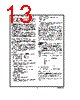
13 / 47 page  5.0 Functional Description (Continued) not changed by these instructions. Consequently, the stack (used with subroutine linkage and interrupts) is always lo- cated in the base segment. The stack pointer will be initial- ized to point at data memory location 006F as a result of re- set. The 128 bytes of RAM contained in the base segment are split between the lower and upper base segments. The first 112 bytes of RAM are resident from address 0000 to 006F in the lower base segment, while the remaining 16 bytes of RAM represent the 16 data memory registers located at ad- dresses 00F0 to 00FF of the upper base segment. No RAM is located at the upper sixteen addresses (0070 to 007F) of the lower base segment. Additional RAM beyond these initial 128 bytes, however, will always be memory mapped in groups of 128 bytes (or less) at the data segment address extensions (XX00 to XX7F) of the lower base segment. The 128 bytes of EERAM in this de- vice are memory mapped at address locations 0100 to 017F. 5.6 SECURITY FEATURE (COP8SER7 only) The program memory array has an associated Security Byte that is located outside of the program address range. This byte can be addressed only from programming mode by a programmer tool. Security is an optional feature and can only be asserted after the memory array has been programmed and verified. A se- cured part will read 00(hex) by a programmer. The part will fail Blank Check and will fail Verify operations. A READ op- eration will fill the programmer’s memory with 00(hex). The Security Byte itself is always readable with value of 00(hex) if unsecure and FF(hex) if secure. 5.7 RESET The devices are initialized when the RESET pin is pulled low. The following occurs upon initialization: Port L: TRI-STATE (High Impedance Input) Port G: TRI-STATE (High Impedance Input) PC: CLEARED to 0000 PSW, CNTRL and ICNTRL registers: CLEARED SIOR: UNAFFECTED after RESET with power already applied RANDOM after RESET at power-on Accumulator, Timer 1: RANDOM after RESET with crystal clock option (power already applied) UNAFFECTED after RESET with R/C clock option (power already applied) RANDOM after RESET at power-on WKEN, WKEDG: CLEARED WKPND: RANDOM SP (Stack Pointer): Initialized to RAM address 06F Hex B and X Pointers: UNAFFECTED after RESET with power already applied RANDOM after RESET at power-on S Register: CLEARED E2CFG: Cleared except the E2BUSY Bit (Bit 1) EERAM: Unaffected ITMR: Cleared RAM: UNAFFECTED after RESET with power already applied RANDOM after RESET at power-on WATCHDOG (if enabled): The device comes out of reset with both the WATCH- DOG logic and the Clock Monitor detector armed, with the WATCHDOG service window bits set and the Clock Monitor bit set. The WATCHDOG and Clock Monitor circuits are in- hibited during reset. The WATCHDOG service window bits being initialized high default to the maximum WATCHDOG service window of 64k t C clock cycles. The Clock Monitor bit being initialized high will cause a Clock Monitor error follow- ing reset if the clock has not reached the minimum specified frequency at the termination of reset. A Clock Monitor error will cause an active low error output on pin G1. This error output will continue until 16 t C–32 tC clock cycles following the clock frequency reaching the minimum specified value, at which time the G1 output will go high. 5.8.1 External Reset The RESET input when pulled low initializes the device. The RESET pin must be held low for a minimum of one instruc- tion cycle to guarantee a valid reset. During Power-Up initial- ization, the user must ensure that the RESET pin is held low until the device is within the specified V CC voltage. An R/C circuit on the RESET pin with a delay 5 times (5x) greater than the power supply rise time is recommended. Reset should also be wide enough to ensure crystal start-up upon Power-Up. RESET may also be used to cause an exit from the HALT mode. A recommended reset circuit for this device is shown in Fig- ure 9. 5.9 OSCILLATOR CIRCUITS These devices can be driven by a clock input on the CKI in- put pin which can be between DC and 10 MHz. The CKO output clock is on pin G7 (crystal configuration). The CKI in- put frequency is divided down by 10 to produce the instruc- tion cycle clock (1/t C ). Figure 10 shows the crystal and R/C oscillator connection diagram. DS100973-14 RC >5x power supply rise time. FIGURE 9. Reset Circuit Using External Reset www.national.com 13 |
|
링크 URL |
| ALLDATASHEET 가 귀하에 도움이 되셨나요? [ DONATE ] |
Alldatasheet는? | 광고문의 | 운영자에게 연락하기 | 개인정보취급방침 | 링크 투 데이터시트 | 링크교환 | 제조사별 검색 All Rights Reserved©Alldatasheet.com |
| Russian : Alldatasheetru.com | Korean : Alldatasheet.co.kr | Spanish : Alldatasheet.es | French : Alldatasheet.fr | Italian : Alldatasheetit.com Portuguese : Alldatasheetpt.com | Polish : Alldatasheet.pl | Vietnamese : Alldatasheet.vn Indian : Alldatasheet.in | Mexican : Alldatasheet.com.mx | British : Alldatasheet.co.uk | New Zealand : Alldatasheet.co.nz |
|
Family Site : ic2ic.com |
icmetro.com |
 Korean ▼
 English
 Chinese
 German
 Japanese
 Russian
 Korean
 Spanish
 French
 Italian
 Portuguese
 Polish
 Vietnamese
 Indian
 Mexican
 British
 New Zealand