|
전자부품 데이터시트 검색엔진 |
|
|
전자부품 데이터시트 검색엔진 |
|
COP8SE 데이터시트(PDF) 11 Page - National Semiconductor (TI) |
|
|
|
|||||||||||||||||||||||||||||
COP8SE 데이터시트(HTML) 11 Page - National Semiconductor (TI) |
|
|
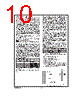
11 / 47 page  4.0 Pin Descriptions (Continued) 5.0 Functional Description The architecture of the devices is a modified Harvard archi- tecture. With the Harvard architecture, the program memory ROM or EPROM is separated from the data store memory (RAM). Program Memory will be referred to as ROM. Both ROM and RAM have their own separate addressing space with separate address buses. The architecture, though based on the Harvard architecture, permits transfer of data from ROM to RAM. 5.1 CPU REGISTERS The CPU can do an 8-bit addition, subtraction, logical or shift operation in one instruction (t C) cycle time. There are six CPU registers: A is the 8-bit Accumulator Register PC is the 15-bit Program Counter Register PU is the upper 7 bits of the program counter (PC) PL is the lower 8 bits of the program counter (PC) B is an 8-bit RAM address pointer, which can be optionally post auto incremented or decremented. X is an 8-bit alternate RAM address pointer, which can be optionally post auto incremented or decremented. S is the 8-bit Segment Address Register used to extend the lower half of the address range (00 to 7F) into 256 data seg- ments of 128 bytes each. SP is the 8-bit stack pointer, which points to the subroutine/ interrupt stack (in RAM). With reset the SP is initialized to RAM address 02F Hex (devices with 64 bytes of RAM), or initialized to RAM address 06F Hex (devices with 128 bytes of RAM). All the CPU registers are memory mapped with the excep- tion of the Accumulator (A) and the Program Counter (PC). 5.2 PROGRAM MEMORY The program memory consists of 4096 Bytes of ROM or 32,768 bytes of OTP EPROM. These bytes may hold pro- gram instructions or constant data (data tables for the LAID instruction, jump vectors for the JID instruction, and interrupt vectors for the VIS instruction). The program memory is ad- dressed by the 15-bit program counter (PC). All interrupts in the device vector to program memory location 0FF Hex. The contents of the program memory read 00 Hex in the erased state. Program execution starts at location 0 after RESET. 5.3 DATA MEMORY The data memory address space includes the on-chip RAM and data registers, the I/O registers (Configuration, Data and Pin), the control registers, the MICROWIRE/PLUS SIO shift register, and the various registers, and counters associated with the timers (with the exception of the IDLE timer). Data memory is addressed directly by the instruction or indirectly by the B, X and SP pointers. The data memory consists of 256 bytes of combined EE- RAM and RAM. Sixteen bytes of RAM are mapped as “reg- isters” at addresses 0F0 to 0FE Hex. These registers can be loaded immediately, and also decremented and tested with the DRSZ (decrement register and skip if zero) instruction. The memory pointer registers X, SP and B are memory mapped into this space at address locations 0FC to 0FE Hex respectively, with the other registers (except 0FF) being available for general usage. The instruction set permits any bit in memory to be set, reset or tested. All I/O and registers (except A and PC) are memory mapped; therefore, I/O bits and register bits can be directly and individually set, reset and tested. The accumula- tor (A) bits can also be directly and individually tested. Note: RAM contents are undefined upon power-up. 5.4 EERAM / NON-VOLATILE MEMORY The devices provide 128 bytes of EERAM in segment 1 for nonvolatile data memory. The data EERAM can be read and written in exactly the same way as the RAM. All instructions that perform read and write operations on the RAM work similarly upon the data EERAM. EERAM write cycles take much more time than reads. During this time, processing continues, but all EERAM accesses are inhibited. The data EERAM contains all 00s when shipped by the factory. A data memory EERAM programming cycle is initiated by an instruction that writes to the EERAM such as X, LD, SBIT and RBIT. The EERAM memory support circuitry sets the E2BUSY flag in the E2CFG register immediately upon begin- ning a data EERAM write cycle. It will be automatically reset by the hardware at the end of the data EERAM write cycle. The application program should test the E2BUSY flag before attempting a read or write operation to the data EERAM. An EERAM read or write operation while an operation is in progress will be ignored and the E2ILRW flag in the E2CFG register will be set to indicate the error status. Once the write operation starts, nothing will stop the write operation, not by resetting the device, and not even turning off the VCC will guarantee the write operation to stop. DS100973-12 FIGURE 6. I/O Port Configurations — Output Mode DS100973-11 FIGURE 7. I/O Port Configurations — Input Mode www.national.com 11 |
|
링크 URL |
| ALLDATASHEET 가 귀하에 도움이 되셨나요? [ DONATE ] |
Alldatasheet는? | 광고문의 | 운영자에게 연락하기 | 개인정보취급방침 | 링크 투 데이터시트 | 링크교환 | 제조사별 검색 All Rights Reserved©Alldatasheet.com |
| Russian : Alldatasheetru.com | Korean : Alldatasheet.co.kr | Spanish : Alldatasheet.es | French : Alldatasheet.fr | Italian : Alldatasheetit.com Portuguese : Alldatasheetpt.com | Polish : Alldatasheet.pl | Vietnamese : Alldatasheet.vn Indian : Alldatasheet.in | Mexican : Alldatasheet.com.mx | British : Alldatasheet.co.uk | New Zealand : Alldatasheet.co.nz |
|
Family Site : ic2ic.com |
icmetro.com |
 Korean ▼
 English
 Chinese
 German
 Japanese
 Russian
 Korean
 Spanish
 French
 Italian
 Portuguese
 Polish
 Vietnamese
 Indian
 Mexican
 British
 New Zealand