|
전자부품 데이터시트 검색엔진 |
|
|
전자부품 데이터시트 검색엔진 |
|
L6986I 데이터시트(PDF) 3 Page - STMicroelectronics |
|
|
|||||||||||||||||||||||||||||
L6986I 데이터시트(HTML) 3 Page - STMicroelectronics |
|
|
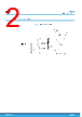
3 / 60 page  2 Pin connection Figure 2. Pin connection (top view) 1 2 3 4 5 6 7 8 16 15 14 13 12 11 10 9 RST VCC SS/INH SYNCH FSW MLF COMP DELAY VBIAS VIN LX LX PGND PGND SGND FB EXPOSED PAD TO SGND+PGND Table 1. Pin description Number Pin Description 1 RST The RST open collector output is driven low when the output voltage is out of regulation. The RST is released after an adjustable time DELAY once the primary output voltage is over the active delay threshold. 2 VCC Connect a ceramic capacitor (≥ 470 nF) to filter internal voltage reference. This pin supplies the embedded analog circuitry. 3 SS / INH An open collector stage can disable the device clamping this pin to GND (INH mode). An internal current generator (4 µA typ.) charges the external capacitor to implement the soft-start. 4 SYNCH The pin features master / slave synchronization. Leave this pin floating when it is not used. 5 FSW A pull-up resistor (E24 series only) to VCC or pull-down to GND selects the switching frequency. Pin strapping is active only before the soft-start phase to minimize the IC consumption. 6 MLF Connect this pin to ground either directly or through a pull-down resistor if the RST threshold should be adjusted (see Table 7). 7 COMP Output of the error amplifier. The designed compensation network is connected at this pin. 8 DELAY An external capacitor connected to this pin sets the time DELAY to assert the rising edge of the RST open collector after the output voltage is over the reset threshold. If this pin is left floating, RST is like a Power Good. 9 FB Primary output voltage sensing 10 SGND Signal GND 11 PGND Power GND 12 PGND Power GND 13 LX Switching node 14 LX Switching node 15 VIN DC input voltage 16 VBIAS Typically connected to the regulated primary output voltage, if it does not exceed 6 V. Otherwise connect it to GND. - Exposed pad Exposed pad must be connected to SGND, PGND L6986I Pin connection DS13647 - Rev 2 page 3/60 |
|
링크 URL |
| ALLDATASHEET 가 귀하에 도움이 되셨나요? [ DONATE ] |
Alldatasheet는? | 광고문의 | 운영자에게 연락하기 | 개인정보취급방침 | 링크 투 데이터시트 | 링크교환 | 제조사별 검색 All Rights Reserved©Alldatasheet.com |
| Russian : Alldatasheetru.com | Korean : Alldatasheet.co.kr | Spanish : Alldatasheet.es | French : Alldatasheet.fr | Italian : Alldatasheetit.com Portuguese : Alldatasheetpt.com | Polish : Alldatasheet.pl | Vietnamese : Alldatasheet.vn Indian : Alldatasheet.in | Mexican : Alldatasheet.com.mx | British : Alldatasheet.co.uk | New Zealand : Alldatasheet.co.nz |
|
Family Site : ic2ic.com |
icmetro.com |
 Korean ▼
 English
 Chinese
 German
 Japanese
 Russian
 Korean
 Spanish
 French
 Italian
 Portuguese
 Polish
 Vietnamese
 Indian
 Mexican
 British
 New Zealand