 |
전자부품 데이터시트 검색엔진 |
|
|
전자부품 데이터시트 검색엔진 |
|
The question interval is too short.
Please try again in a few seconds.

Hello, Please ask a question about DSP56367 Datasheet
# Example questions:
➢ Identify at least three different types of memory components present in this system architecture and their respective sizes as stated in the diagram.
➢ What is the role of the 'external address bus switch' and 'external data bus switch' in relation to the 'dram & sram bus interface'?
➢ What is the primary function of the 'dma unit' as indicated in the diagram?
| Part No. | DSP56367 |
| Manufacturer | FREESCALE |
| Size | 1Mb |
| Pages | 100 pages |
| Description | 24-Bit Audio Digital Signal Processor |


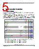
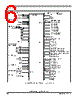


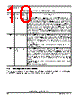
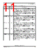


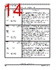


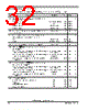

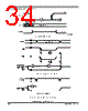


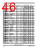


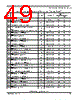
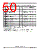

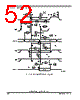


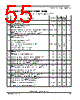

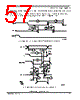


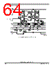


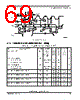


1. Overall Architecture & Key Components
️· DSP Core: The diagram heavily revolves around what appears to be a DSP core, indicated by the presence of Arithmetic Logic Units (ALUs), multipliers, adders, and related logic.
️· Memory Hierarchy: There's a clear emphasis on a memory system. This includes:
- On-Chip ROM: A read-only memory for storing program code.
- On-Chip RAM: Random Access Memory for data storage during processing.
- External Memory Interface: Logic to access external memory (likely SDRAM or similar).
️· Peripheral Interfaces: Numerous peripheral interfaces are present, suggesting a rich set of I/O capabilities.
️· Bus Architecture: A complex bus structure is implied, handling data flow between different components.
️· Control Logic: Various controllers and logic units orchestrate the operation of the system.
️· Multiple O_EB components Numerous components indicated as O_EB. This is likely some sort of output enable signal or output component.
2. Detailed Breakdown of Components
Let's categorize the blocks, as much as possible, given the density:
️· Processing Units:
- ALUs (Arithmetic Logic Units): For performing arithmetic and logical operations. Multiple ALUs indicate parallel processing capabilities.
- Multipliers: For fast multiplication, a core operation in DSP.
- Adders/Subtractors: For fast addition and subtraction.
- Shifters: For bit manipulation and multiplication/division by powers of 2.
️· Memory Components:
- ROM (Read-Only Memory): Stores program instructions.
- RAM (Random Access Memory): For data storage and manipulation. On-chip and off-chip RAM are distinguished.
- Memory Controllers: Manage access to RAM, implementing refresh cycles and error correction.
️· Control Units & Logic:
- Program Counter (PC): Keeps track of the address of the next instruction to be executed.
- Instruction Decoder: Decodes instructions and generates control signals.
- Sequencer: Generates micro-sequences to control the operation of the ALU and other functional units.
- Interrupt Controller: Handles interrupts from external devices.
️· Peripheral Interfaces: These are numerous and indicate a versatile I/O system. Some potential interfaces include:
- Serial Ports (UART, SPI, I2C): For communication with other devices.
- Parallel Ports: For high-speed data transfer.
- Analog-to-Digital Converters (ADCs): Convert analog signals to digital.
- Digital-to-Analog Converters (DACs): Convert digital signals to analog.
- Timers/Counters: For generating time delays and counting events.
️· Bus Components:
- Address Bus: Carries memory addresses.
- Data Bus: Carries data between components.
- Control Bus: Carries control signals.
3. Key Architectural Features & Implications
️· Parallelism: The multiple ALUs, multipliers, and memory banks suggest significant parallel processing capabilities. This is crucial for demanding real-time applications.
️· Pipelining: The design likely incorporates pipelining to increase throughput by overlapping the execution of multiple instructions.
️· Real-Time Processing: The presence of timers, interrupt controllers, and fast memory access suggests a design optimized for real-time signal processing.
️· Configurability/Flexibility: The range of peripherals and bus interfaces suggests a highly configurable and versatile system.
️· Multiple O_EB signal: The numerous O_EB components suggest these are signals enabling output processing.
4. Potential Applications
Based on the architecture, this DSP/system could be used for a wide range of applications, including:
️· Audio Processing: Digital signal processing for audio equalization, noise reduction, and effects.
️· Image Processing: Image filtering, edge detection, and other image manipulation tasks.
️· Communications: Modulation, demodulation, and encoding/decoding of signals.
️· Motor Control: Precise control of electric motors.
️· Industrial Automation: Data acquisition, control, and monitoring.
Limitations and Disclaimers:
️· Lack of Context: Without knowing the specific device or system this diagram represents, it is difficult to give a fully accurate interpretation.
️· Abbreviations: Many abbreviations are used. A complete understanding would require a key or datasheet.
️· Abstraction Level: The level of abstraction is not clear. Some blocks may represent entire subsystems.
️· Diagram Clarity: It is difficult to follow some connections due to the diagram's density and complexity.
1. Overall Architecture & Key Components
️· DSP Core: The diagram heavily revolves around what appears to be a DSP core, indicated by the presence of Arithmetic Logic Units (ALUs), multipliers, adders, and related logic.
️· Memory Hierarchy: There's a clear emphasis on a memory system. This includes:
- On-Chip ROM: A read-only memory for storing program code.
- On-Chip RAM: Random Access Memory for data storage during processing.
- External Memory Interface: Logic to access external memory (likely SDRAM or similar).
️· Peripheral Interfaces: Numerous peripheral interfaces are present, suggesting a rich set of I/O capabilities.
️· Bus Architecture: A complex bus structure is implied, handling data flow between different components.
️· Control Logic: Various controllers and logic units orchestrate the operation of the system.
️· Multiple O_EB components Numerous components indicated as O_EB. This is likely some sort of output enable signal or output component.
2. Detailed Breakdown of Components
Let's categorize the blocks, as much as possible, given the density:
️· Processing Units:
- ALUs (Arithmetic Logic Units): For performing arithmetic and logical operations. Multiple ALUs indicate parallel processing capabilities.
- Multipliers: For fast multiplication, a core operation in DSP.
- Adders/Subtractors: For fast addition and subtraction.
- Shifters: For bit manipulation and multiplication/division by powers of 2.
️· Memory Components:
- ROM (Read-Only Memory): Stores program instructions.
- RAM (Random Access Memory): For data storage and manipulation. On-chip and off-chip RAM are distinguished.
- Memory Controllers: Manage access to RAM, implementing refresh cycles and error correction.
️· Control Units & Logic:
- Program Counter (PC): Keeps track of the address of the next instruction to be executed.
- Instruction Decoder: Decodes instructions and generates control signals.
- Sequencer: Generates micro-sequences to control the operation of the ALU and other functional units.
- Interrupt Controller: Handles interrupts from external devices.
️· Peripheral Interfaces: These are numerous and indicate a versatile I/O system. Some potential interfaces include:
- Serial Ports (UART, SPI, I2C): For communication with other devices.
- Parallel Ports: For high-speed data transfer.
- Analog-to-Digital Converters (ADCs): Convert analog signals to digital.
- Digital-to-Analog Converters (DACs): Convert digital signals to analog.
- Timers/Counters: For generating time delays and counting events.
️· Bus Components:
- Address Bus: Carries memory addresses.
- Data Bus: Carries data between components.
- Control Bus: Carries control signals.
3. Key Architectural Features & Implications
️· Parallelism: The multiple ALUs, multipliers, and memory banks suggest significant parallel processing capabilities. This is crucial for demanding real-time applications.
️· Pipelining: The design likely incorporates pipelining to increase throughput by overlapping the execution of multiple instructions.
️· Real-Time Processing: The presence of timers, interrupt controllers, and fast memory access suggests a design optimized for real-time signal processing.
️· Configurability/Flexibility: The range of peripherals and bus interfaces suggests a highly configurable and versatile system.
️· Multiple O_EB signal: The numerous O_EB components suggest these are signals enabling output processing.
4. Potential Applications
Based on the architecture, this DSP/system could be used for a wide range of applications, including:
️· Audio Processing: Digital signal processing for audio equalization, noise reduction, and effects.
️· Image Processing: Image filtering, edge detection, and other image manipulation tasks.
️· Communications: Modulation, demodulation, and encoding/decoding of signals.
️· Motor Control: Precise control of electric motors.
️· Industrial Automation: Data acquisition, control, and monitoring.
Limitations and Disclaimers:
️· Lack of Context: Without knowing the specific device or system this diagram represents, it is difficult to give a fully accurate interpretation.
️· Abbreviations: Many abbreviations are used. A complete understanding would require a key or datasheet.
️· Abstraction Level: The level of abstraction is not clear. Some blocks may represent entire subsystems.
️· Diagram Clarity: It is difficult to follow some connections due to the diagram's density and complexity.
| Part No. | DSP56367 |
| Manufacturer | FREESCALE |
| Size | 1Mb |
| Pages | 100 pages |
| Description | 24-Bit Audio Digital Signal Processor |
| ALLDATASHEET 가 귀하에 도움이 되셨나요? [ DONATE ] |
Alldatasheet는? | 광고문의 | 운영자에게 연락하기 | 개인정보취급방침 | 링크 투 데이터시트 | 링크교환 | 제조사별 검색 All Rights Reserved©Alldatasheet.com |
| Russian : Alldatasheetru.com | Korean : Alldatasheet.co.kr | Spanish : Alldatasheet.es | French : Alldatasheet.fr | Italian : Alldatasheetit.com Portuguese : Alldatasheetpt.com | Polish : Alldatasheet.pl | Vietnamese : Alldatasheet.vn Indian : Alldatasheet.in | Mexican : Alldatasheet.com.mx | British : Alldatasheet.co.uk | New Zealand : Alldatasheet.co.nz |
|
Family Site : ic2ic.com |
icmetro.com |
 Korean ▼
  English
 Chinese
 German
 Japanese
 Russian
 Spanish
 French
 Italian
 Portuguese
 Polish
 Vietnamese
 Indian
 Mexican
 British
 New Zealand