|
전자부품 데이터시트 검색엔진 |
|
|
전자부품 데이터시트 검색엔진 |
|
DSP56367 데이터시트(PDF) 56 Page - Freescale Semiconductor, Inc |
|
|
|||||||||||||||||||||||||||||
DSP56367 데이터시트(HTML) 56 Page - Freescale Semiconductor, Inc |
|
|
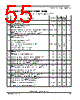
56 / 100 page  Parallel Host Interface (HDI08) Timing DSP56367 Technical Data, Rev. 2.1 3-32 Freescale Semiconductor 332 HCS assertion to output data valid — — 19.1 ns 333 HCS hold time after data strobe deassertion9 —0.0 — ns 334 Address (AD7–AD0) setup time before HAS deassertion (HMUX=1) — 4.7 — ns 335 Address (AD7–AD0) hold time after HAS deassertion (HMUX=1) — 3.3 — ns 336 A10–A8 (HMUX=1), A2–A0 (HMUX=0), HR/W setup time before data strobe assertion9 •Read • Write —0 4.7 — — ns 337 A10–A8 (HMUX=1), A2–A0 (HMUX=0), HR/W hold time after data strobe deassertion9 —3.3 — ns 338 Delay from read data strobe deassertion to host request assertion for “Last Data Register” read4, 5, 10 TC 6.7 — ns 339 Delay from write data strobe deassertion to host request assertion for “Last Data Register” write5, 8, 10 2 × TC 13.4 — ns 340 Delay from data strobe assertion to host request deassertion for “Last Data Register” read or write (HROD = 0)5, 9, 10 — — 19.1 ns 341 Delay from data strobe assertion to host request deassertion for “Last Data Register” read or write (HROD = 1, open drain Host Request)5, 9, 10, 11 — — 300.0 ns 342 Delay from DMA HACK deassertion to HOREQ assertion • For “Last Data Register” read5 • For “Last Data Register” write5 • For other cases 2 × TC + 19.1 1.5 × TC + 19.1 32.5 29.2 0.0 — — — ns 343 Delay from DMA HACK assertion to HOREQ deassertion •HROD = 05 — — 20.2 ns 344 Delay from DMA HACK assertion to HOREQ deassertion for “Last Data Register” read or write • HROD = 1, open drain Host Request5, 11 — — 300.0 ns 1 See Host Port Usage Considerations in the DSP56367 User’s Manual. 2 In the timing diagrams below, the controls pins are drawn as active low. The pin polarity is programmable. 3 V CC = 1.8 V ± 5%; TJ = –40°C to +95°C, CL = 50 pF 4 The read data strobe is HRD in the dual data strobe mode and HDS in the single data strobe mode. 5 The “last data register” is the register at address $7, which is the last location to be read or written in data transfers. 6 This timing is applicable only if a read from the “last data register” is followed by a read from the RXL, RXM, or RXH registers without first polling RXDF or HREQ bits, or waiting for the assertion of the HOREQ signal. 7 This timing is applicable only if two consecutive reads from one of these registers are executed. 8 The write data strobe is HWR in the dual data strobe mode and HDS in the single data strobe mode. Table 3-15 Host Interface (HDI08) Timing1, 2, 3 (continued) No. Characteristics Expression 150 MHz Unit Min Max |
|
링크 URL |
| ALLDATASHEET 가 귀하에 도움이 되셨나요? [ DONATE ] |
Alldatasheet는? | 광고문의 | 운영자에게 연락하기 | 개인정보취급방침 | 링크 투 데이터시트 | 링크교환 | 제조사별 검색 All Rights Reserved©Alldatasheet.com |
| Russian : Alldatasheetru.com | Korean : Alldatasheet.co.kr | Spanish : Alldatasheet.es | French : Alldatasheet.fr | Italian : Alldatasheetit.com Portuguese : Alldatasheetpt.com | Polish : Alldatasheet.pl | Vietnamese : Alldatasheet.vn Indian : Alldatasheet.in | Mexican : Alldatasheet.com.mx | British : Alldatasheet.co.uk | New Zealand : Alldatasheet.co.nz |
|
Family Site : ic2ic.com |
icmetro.com |
 Korean ▼
 English
 Chinese
 German
 Japanese
 Russian
 Korean
 Spanish
 French
 Italian
 Portuguese
 Polish
 Vietnamese
 Indian
 Mexican
 British
 New Zealand