|
전자부품 데이터시트 검색엔진 |
|
|
전자부품 데이터시트 검색엔진 |
|
MPC8321EVRADDC 데이터시트(PDF) 65 Page - Freescale Semiconductor, Inc |
|
|
|||||||||||||||||||||||||||||
MPC8321EVRADDC 데이터시트(HTML) 65 Page - Freescale Semiconductor, Inc |
|
|
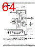
65 / 82 page  MPC8323E PowerQUICC II Pro Integrated Communications Processor Family Hardware Specifications, Rev. 4 Freescale Semiconductor 65 Clocking 22.1 Clocking in PCI Host Mode When the MPC8323E is configured as a PCI host device (RCWH[PCIHOST] = 1), CLKIN is its primary input clock. CLKIN feeds the PCI clock divider ( ÷2) and the PCI_SYNC_OUT and PCI_CLK_OUT multiplexors. The CFG_CLKIN_DIV configuration input selects whether CLKIN or CLKIN/2 is driven out on the PCI_SYNC_OUT signal. PCI_SYNC_OUT is connected externally to PCI_SYNC_IN to allow the internal clock subsystem to synchronize to the system PCI clocks. PCI_SYNC_OUT must be connected properly to PCI_SYNC_IN, with equal delay to all PCI agent devices in the system. 22.1.1 PCI Clock Outputs (PCI_CLK_OUT[0:2]) When the MPC8323E is configured as a PCI host, it provides three separate clock output signals, PCI_CLK_OUT[0:2], for external PCI agents. When the device comes out of reset, the PCI clock outputs are disabled and are actively driven to a steady low state. Each of the individual clock outputs can be enabled (enable toggling of the clock) by setting its corresponding OCCR[PCICOEn] bit. All output clocks are phase-aligned to each other. 22.2 Clocking in PCI Agent Mode When the MPC8323E is configured as a PCI agent device, PCI_CLK is the primary input clock. In agent mode, the CLKIN signal should be tied to GND, and the clock output signals, PCI_CLK_OUTn and PCI_SYNC_OUT, are not used. 22.3 System Clock Domains As shown in Figure 43, the primary clock input (frequency) is multiplied up by the system phase-locked loop (PLL) and the clock unit to create three major clock domains: • The coherent system bus clock (csb_clk) • The QUICC Engine clock (ce_clk) • The internal clock for the DDR controller (ddr_clk) • The internal clock for the local bus controller (lb_clk) The csb_clk frequency is derived from a complex set of factors that can be simplified into the following equation: csb_clk = [PCI_SYNC_IN × (1 + ~CFG_CLKIN_DIV)] × SPMF In PCI host mode, PCI_SYNC_IN × (1 + ~CFG_CLKIN_DIV) is the CLKIN frequency. The csb_clk serves as the clock input to the e300c2 core. A second PLL inside the core multiplies up the csb_clk frequency to create the internal clock for the core (core_clk). The system and core PLL multipliers are selected by the SPMF and COREPLL fields in the reset configuration word low (RCWL) which is loaded at power-on reset or by one of the hard-coded reset options. See the “Reset Configuration” section in the MPC8323E PowerQUICC II Pro Communications Processor Reference Manual for more information. |
|
링크 URL |
| ALLDATASHEET 가 귀하에 도움이 되셨나요? [ DONATE ] |
Alldatasheet는? | 광고문의 | 운영자에게 연락하기 | 개인정보취급방침 | 링크 투 데이터시트 | 링크교환 | 제조사별 검색 All Rights Reserved©Alldatasheet.com |
| Russian : Alldatasheetru.com | Korean : Alldatasheet.co.kr | Spanish : Alldatasheet.es | French : Alldatasheet.fr | Italian : Alldatasheetit.com Portuguese : Alldatasheetpt.com | Polish : Alldatasheet.pl | Vietnamese : Alldatasheet.vn Indian : Alldatasheet.in | Mexican : Alldatasheet.com.mx | British : Alldatasheet.co.uk | New Zealand : Alldatasheet.co.nz |
|
Family Site : ic2ic.com |
icmetro.com |
 Korean ▼
 English
 Chinese
 German
 Japanese
 Russian
 Korean
 Spanish
 French
 Italian
 Portuguese
 Polish
 Vietnamese
 Indian
 Mexican
 British
 New Zealand