|
전자부품 데이터시트 검색엔진 |
|
|
전자부품 데이터시트 검색엔진 |
|
MPC8321EVRADDC 데이터시트(PDF) 66 Page - Freescale Semiconductor, Inc |
|
|
|||||||||||||||||||||||||||||
MPC8321EVRADDC 데이터시트(HTML) 66 Page - Freescale Semiconductor, Inc |
|
|
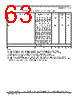
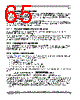
66 / 82 page  MPC8323E PowerQUICC II Pro Integrated Communications Processor Family Hardware Specifications, Rev. 4 66 Freescale Semiconductor Clocking The ce_clk frequency is determined by the QUICC Engine PLL multiplication factor (RCWL[CEPMF) and the QUICC Engine PLL division factor (RCWL[CEPDF]) according to the following equation: When CLKIN is the primary input clock, ce_clk = (primary clock input × CEPMF) ÷ (1 + CEPDF) When PCI_CLK is the primary input clock, ce_clk = [primary clock input × CEPMF × (1 + ~CFG_CLKIN_DIV)] ÷ (1 + CEPDF) See the “QUICC Engine PLL Multiplication Factor” section and the “QUICC Engine PLL Division Factor” section in the MPC8323E PowerQUICC II Pro Communications Processor Reference Manual for more information. The DDR SDRAM memory controller operates with a frequency equal to twice the frequency of csb_clk. Note that ddr_clk is not the external memory bus frequency; ddr_clk passes through the DDR clock divider ( ÷2) to create the differential DDR memory bus clock outputs (MCK and MCK). However, the data rate is the same frequency as ddr_clk. The local bus memory controller operates with a frequency equal to the frequency of csb_clk. Note that lbc_clk is not the external local bus frequency; lbc_clk passes through the LBC clock divider to create the external local bus clock outputs (LSYNC_OUT and LCLK[0:2]). The LBC clock divider ratio is controlled by LCRR[CLKDIV]. See the “LBC Bus Clock and Clock Ratios” section in the MPC8323E PowerQUICC II Pro Communications Processor Reference Manual for more information. In addition, some of the internal units may be required to be shut off or operate at lower frequency than the csb_clk frequency. These units have a default clock ratio that can be configured by a memory mapped register after the device comes out of reset. Table 56 specifies which units have a configurable clock frequency. Refer to the “System Clock Control Register (SCCR)” section in the MPC8323E PowerQUICC II Pro Communications Processor Reference Manual for a detailed description. NOTE Setting the clock ratio of these units must be performed prior to any access to them. Table 57 provides the operating frequencies for the 8323E PBGA under recommended operating conditions (see Table 2). Table 56. Configurable Clock Units Unit Default Frequency Options Security core, I2C, SAP, TPR csb_clk Off, csb_clk/2, csb_clk/3 PCI and DMA complex csb_clk Off, csb_clk Table 57. Operating Frequencies for PBGA Characteristic1 Max Operating Frequency Unit e300 core frequency ( core_clk)333 MHz Coherent system bus frequency ( csb_clk)133 MHz QUICC Engine frequency ( ce_clk)200 MHz |
|
링크 URL |
| ALLDATASHEET 가 귀하에 도움이 되셨나요? [ DONATE ] |
Alldatasheet는? | 광고문의 | 운영자에게 연락하기 | 개인정보취급방침 | 링크 투 데이터시트 | 링크교환 | 제조사별 검색 All Rights Reserved©Alldatasheet.com |
| Russian : Alldatasheetru.com | Korean : Alldatasheet.co.kr | Spanish : Alldatasheet.es | French : Alldatasheet.fr | Italian : Alldatasheetit.com Portuguese : Alldatasheetpt.com | Polish : Alldatasheet.pl | Vietnamese : Alldatasheet.vn Indian : Alldatasheet.in | Mexican : Alldatasheet.com.mx | British : Alldatasheet.co.uk | New Zealand : Alldatasheet.co.nz |
|
Family Site : ic2ic.com |
icmetro.com |
 Korean ▼
 English
 Chinese
 German
 Japanese
 Russian
 Korean
 Spanish
 French
 Italian
 Portuguese
 Polish
 Vietnamese
 Indian
 Mexican
 British
 New Zealand