|
전자부품 데이터시트 검색엔진 |
|
|
전자부품 데이터시트 검색엔진 |
|
PIFE32251B-R68MS 데이터시트(PDF) 19 Page - Texas Instruments |
|
|
|||||||||||||||||||||||||||||
PIFE32251B-R68MS 데이터시트(HTML) 19 Page - Texas Instruments |
|
|
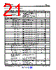
19 / 157 page  19 TPS650830 www.ti.com SLVSCF4A – DECEMBER 2014 – REVISED JULY 2016 Submit Documentation Feedback Product Folder Links: TPS650830 Specifications Copyright © 2014–2016, Texas Instruments Incorporated Electrical Characteristics (continued) Over recommended free-air temperature range and over recommended input voltage range (typical at an ambient temperature range of 25°C) (unless otherwise noted) PARAMETER TEST CONDITIONS MIN TYP MAX UNIT IO (LDO3V) Output current Maximum current for external user is limited 40 mA 40 mA ISC (LDO3V) Output circuit current limit Measured at 90% of the regulation voltage 75 mA Line regulation VO(LDO3V) Line regulation for regulator over operating voltage range VIN = 5.4 V to 21 V, Measured as (ΔVO(LDO3V)/VO(LDO3V)) over the operating range with 20-mA load current. measured at LDO3V pin with respect to AGND pin 0.5% Load regulation VO(LDO3V) Load regulation for regulator over operating current range VIN = 7.4 Measured as (ΔVO(LDO3V)/VO(LDO3V)) over this operating range with 0-mA to 50-mA load current. measured at LDO3V pin with respect to AGND pin 0.5% CO (LDO3V) External output capacitance range after derating Actual capacitance after derating. ex: 2.7- µF capacitance, then use a 4.7-µF capacitor with 60% deratingat 3.3 V. 2.2 4.7 10 μF TR (LDO3V) Rise time Measured from 5% to 95% of the output voltage with 2.2 μF 300 450 μs CONTROL - INPUT/ OUTPUT BUFFERS CONTROL - DDR_VTT_CTRL (Intel external connection DDR_VTT_CTRL) - 1 V logic, tolerates 3 V VIL_DDR_VTT_CTR L DDR_VTT_CTRL input low voltage Input low voltage threshold 0.49 V VIH_DDR_VTT_CTR L DDR_VTT_CTRL input high voltage Input high voltage threshold 0.61 V VHYST_DDR_VTT_ CTRL DDR_VTT_CTRL hysteresis voltage Hysteresis voltage 70 mV Ileakage_DDR_VTT_ CTRL DDR_VTT_CTRL input current Input current, Clamped to 1.0 V 0.01 0.2 μA CONTROL - INPUT TTL BUFFERS (ALL INPUT PINS), (DEFAULT: SHUTDOWNZ, STANDBYZ, ENLVA, EN3V3SW, EN5VSW, ENVR1, ENVR2, ENVR3, ENVR4, ENVR5, ENA. ENB, ENC, END, ENE, ENF, ENG, ENH), (OPTIONAL: VSA, VSB, VSC, VSD, VSE, VSF, VSG, VSH, ENLVA) VIL_INPUTS Input low voltage 0.4 V VIH_INPUTS Input high voltage 1.2 V VHYST_INPUTS Hysteresis voltage 300 mV Ileakage_INPUTS Input current Clamped on 3.3 V 0.01 0.3 μA VIL_PWRBTNZ Input low voltage for PWRBTNZ 0.4 V VIH_PWRBTNZ Input high voltage for PWRBTNZ Internal 5-kΩ pull-up resistor between PWRBTNZ pin and VDDIO 1.6 V VHYST_PWRBTNZ Hysteresis voltage for PWRBTNZ 580 mV IOutput_PWRBTNZ Output current for PWRBTNZ when power button is pressed to close and pulling PWRBTNZ to GND. PWRBTNZ = GND, Internal 5-kΩ pull-up resistor between PWRBTNZ pin and VDDIO 660 790 μA TEC_ONOFFZ_Debo uinc_0e EC_ONOFFZ_Debounce time, 0 setting Time set to 0 ms, Measured from 0.5% PWBTNZ rising to 5% of the EC_ONOFFZ output 0 ms TEC_ONOFFZ_Debo uinc_30e EC_ONOFFZ_Debounce time, 30 ms setting Time set to 30 ms, Measured from 0.5% PWBTNZ rising to 5% of the EC_ONOFFZ output 30 ms CONTROL - VDDIO DOMAIN PUSH-PULL OUTPUTS, (RESETZ, 1HZ, DS3_VREN), (Optional: PGVR1, PGVR2, PGVR3, PGVR4, PGVR5) VPP Pull-up output voltage supply Pulled-Up to VDDIO pin which should by tied to LDO3V pin = 3.3 V VDDIO V VOL_PP Low level output voltage IOL = 3 mA 0.6 V |
|
링크 URL |
| ALLDATASHEET 가 귀하에 도움이 되셨나요? [ DONATE ] |
Alldatasheet는? | 광고문의 | 운영자에게 연락하기 | 개인정보취급방침 | 링크 투 데이터시트 | 링크교환 | 제조사별 검색 All Rights Reserved©Alldatasheet.com |
| Russian : Alldatasheetru.com | Korean : Alldatasheet.co.kr | Spanish : Alldatasheet.es | French : Alldatasheet.fr | Italian : Alldatasheetit.com Portuguese : Alldatasheetpt.com | Polish : Alldatasheet.pl | Vietnamese : Alldatasheet.vn Indian : Alldatasheet.in | Mexican : Alldatasheet.com.mx | British : Alldatasheet.co.uk | New Zealand : Alldatasheet.co.nz |
|
Family Site : ic2ic.com |
icmetro.com |
 Korean ▼
 English
 Chinese
 German
 Japanese
 Russian
 Korean
 Spanish
 French
 Italian
 Portuguese
 Polish
 Vietnamese
 Indian
 Mexican
 British
 New Zealand