|
전자부품 데이터시트 검색엔진 |
|
|
전자부품 데이터시트 검색엔진 |
|
PIFE32251B-R68MS 데이터시트(PDF) 24 Page - Texas Instruments |
|
|
|||||||||||||||||||||||||||||
PIFE32251B-R68MS 데이터시트(HTML) 24 Page - Texas Instruments |
|
|
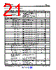
24 / 157 page  24 TPS650830 SLVSCF4A – DECEMBER 2014 – REVISED JULY 2016 www.ti.com Submit Documentation Feedback Product Folder Links: TPS650830 Specifications Copyright © 2014–2016, Texas Instruments Incorporated Electrical Characteristics (continued) Over recommended free-air temperature range and over recommended input voltage range (typical at an ambient temperature range of 25°C) (unless otherwise noted) PARAMETER TEST CONDITIONS MIN TYP MAX UNIT Switching frequency (7.4 V) PWM Mode (NVDC# = 3.3 V = programmed to low switching frequency) 379 500 550 kHz PWM Mode (NVDC# = GND = programmed to high switching frequency) 715 800 865 kHz Soft-Start total turn-on time (start- up time + output ramp-up time) Time to start switching from enable to 95% of VO(Min), Continuous slope (no slope reversal) 770 876 1000 μs Soft-Start delay time Delay time from enable to first switching pulse. 120 136 150 μs Soft-Start ramp-up time From first switching pulse to 95% of VO(Min), Continuous slope (no slope reversal). 650 740 850 μs DVS total fall time (delay time + output ramp-down time) Time to start switching from enable to 5% of VO(Min), Continuous slope (no slope reversal). 56 61.25 68.5 μs DVS delay time for falling edge DVS delay time from when STANDBYZ (SLP_S0#) changes from High to Low, until the output voltage begins to fall. 1 1.25 1.5 μs DVS ramp time for falling edge From first switching pulse to 5% of VO(Min), Continuous slope (no slope reversal). Total ramp time = ((Vout_high - Vout_low) / slew_rate). For Vout change = 300 mV 55 60 67 μs DVS slew rate for falling edge DVS falling edge slew rate for VVOUT to change from the upper target to the lower target after STANDBYZ (SLP_S0#) changes from High to Low. Total ramp time = ((Vout_high - Vout_low) / slew_rate) 4.5 5 5.5 mV / μs DVS total rise time (delay time + output ramp-rise time) Time to start switching from enable to 95% of VO(Min), Continuous slope (no slope reversal). 56 61.25 68.5 μs DVS delay time for rising edge DVS delay time from when STANDBYZ (SLP_S0#) changes from Low to High, until the output voltage begins to rise. 1 1.25 1.5 μs DVS ramp time for rising edge From first switching pulse to 95% of VO(Min), Continuous slope (no slope reversal). Total ramp time = ((Vout_high - Vout_low) / slew_rate). For Vout change = 300 mV 55 60 67 μs DVS slew rate for rising edge DVS rising edge slew rate for VVOUT to change from the lower target to the upper target after STANDBYZ (SLP_S0#) changes from Low to High. Total ramp time = ((Vout_high - Vout_low) / slew_rate) 4.5 5 5.5 mV / μs Decay exit Total turn-on time (delay time + output ramp-up time) Time to start switching from enable to 95% of VO(Min), Continuous slope (no slope reversal). 69 79 99 μs Decay exit delay time for rising edge Decay delay time from when STANDBYZ (SLP_S0#) changes from Low to High, until the output voltage begins to rise. 10 12 16 μs Decay exit ramp time for rising edge From first switching pulse to 95% of VO(Min), Continuous slope (no slope reversal). Total ramp time = ((Vout_high - 0 V) / slew_rate). For Vout target = 1.00 V. 59 67 83 μs |
|
링크 URL |
| ALLDATASHEET 가 귀하에 도움이 되셨나요? [ DONATE ] |
Alldatasheet는? | 광고문의 | 운영자에게 연락하기 | 개인정보취급방침 | 링크 투 데이터시트 | 링크교환 | 제조사별 검색 All Rights Reserved©Alldatasheet.com |
| Russian : Alldatasheetru.com | Korean : Alldatasheet.co.kr | Spanish : Alldatasheet.es | French : Alldatasheet.fr | Italian : Alldatasheetit.com Portuguese : Alldatasheetpt.com | Polish : Alldatasheet.pl | Vietnamese : Alldatasheet.vn Indian : Alldatasheet.in | Mexican : Alldatasheet.com.mx | British : Alldatasheet.co.uk | New Zealand : Alldatasheet.co.nz |
|
Family Site : ic2ic.com |
icmetro.com |
 Korean ▼
 English
 Chinese
 German
 Japanese
 Russian
 Korean
 Spanish
 French
 Italian
 Portuguese
 Polish
 Vietnamese
 Indian
 Mexican
 British
 New Zealand